'Fule nouhan' bi-directional write/erase flash memory in low voltage

A low-voltage, memory technology, applied in the field of low-voltage bidirectional Fowler Nohan write/erase flash memory, which can solve the problems of large chip area and high production cost

Inactive Publication Date: 2004-03-10
POWERCHIP SEMICON CORP
View PDF0 Cites 4 Cited by
  • Summary
  • Abstract
  • Description
  • Claims
  • Application Information

AI Technical Summary

Problems solved by technology

In addition, it is known that flash memory occupies a large chip area, so the production cost is relatively high

Method used


Image

  • 'Fule nouhan' bi-directional write/erase flash memory in low voltage
  • 'Fule nouhan' bi-directional write/erase flash memory in low voltage
  • 'Fule nouhan' bi-directional write/erase flash memory in low voltage

Examples


Embodiment Construction

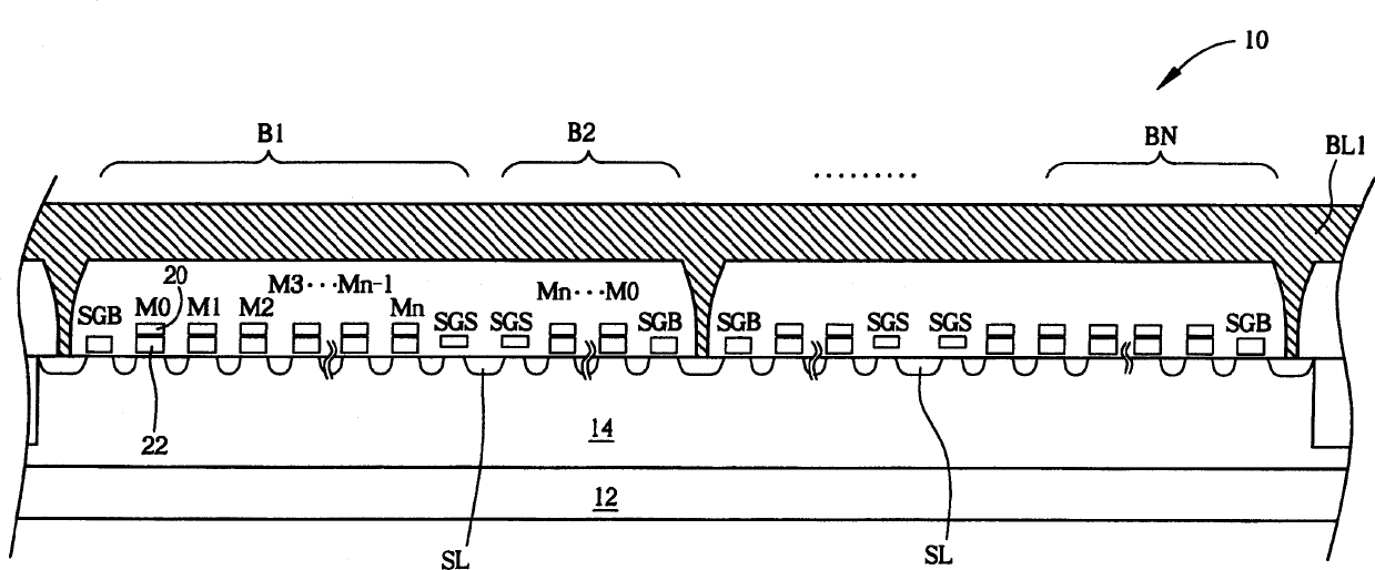
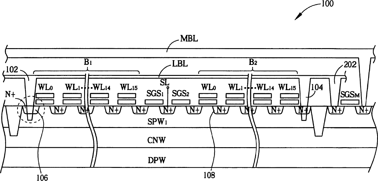
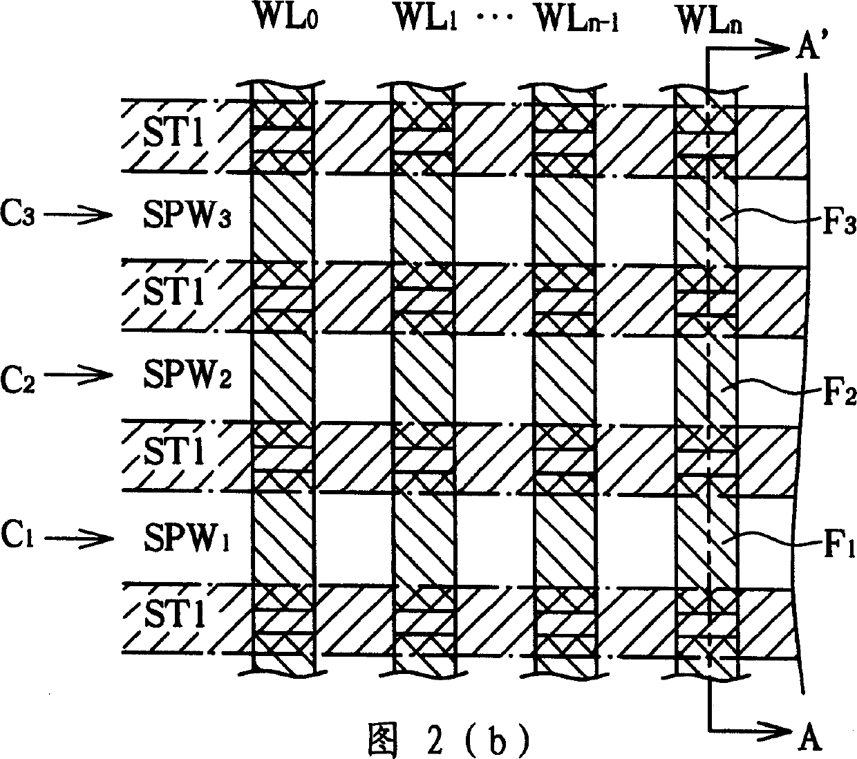
[0036] Please refer to FIG. 2( a ). FIG. 2( a ) is a partial cross-sectional structural diagram of the EEPROM 100 according to the first embodiment of the present invention. As shown in FIG. 2, EEPROM 100 is a low-voltage bidirectional FN write / erase NAND flash memory array structure, including a P-type semiconductor deep well (deep P-well, hereinafter referred to as DPW), and a memory cell sharing N-type well (cell N-Well, hereinafter referred to as CNW), a shallow P-well (shallow P-well, hereinafter referred to as SPW) arranged in parallel and isolated from each other by a shallow trench insulation region, used as a buried Type bit line (buried bit line). In Fig. 2(a), only one of the multiple rows of SPWs is displayed: SPW1. A plurality of NAND cell blocks are arranged in the same column and formed on SPW1, and a local bit line (hereinafter referred to as LBL) is arranged above the plurality of NAND cell blocks. For the convenience of describing the present invention, onl...


PUM


Abstract

The memory includes a substrate and following structure. Common doping trap of first conduction type storage unit is formed on the substrate. Insulated each other multiple second conduction type embedded bit lines is formed on common doping trap of the storage unit. Multiple storage regional blocks arranged in series are formed on single line in multiple embedded bit lines. Each multiple storage regional block contains at least one piece of storage transistor, which includes stacked grid electrodes, source electrode and drain electrode. Being parallel spanned above multiple storage regional blocks in series, the regional bit line through contact plug is contacted to drain electrode electrically. Moreover, electrical short circuit is formed between the contact plug and inferior embedded bit line. The invention has low power expenditure and compatible operation mode. Thus, high-speed program flash memory and high-density data flash memory can be integrated in single chip.

Description

technical field [0001] The present invention relates to a kind of nonvolatile (nonvolatile) memory, especially a kind of low-voltage two-way (bi-directional) Fleur Nohan (FN) write / erase flash memory, has low power consumption, compatible In the operation mode, features such as high-speed code flash memory (codeflash) and high-density data flash memory (data flash) can be integrated on a single chip at the same time. Background technique [0002] In recent years, as the demand for portable (portable) electronic products increases, the technology and market application of flash (flash) memory or electrically erasable programmable read-only memory (electrically erasable programmable read-only memory, hereinafter referred to as EEPROM) are also increasing. Mature and expand. These portable electronic products include negatives of digital cameras, mobile phones, video game apparatuses, memories of personal digital assistants (PDAs), telephone answering devices, programmable ICs...

Claims


Application Information

Patent Timeline
Patent Type & Authority Applications(China)
IPC IPC(8): G11C11/34H01L27/10
Inventor 杨青松沈士杰徐清祥
Owner POWERCHIP SEMICON CORP
Why Eureka
Try Eureka