Chip transfer method and apparatus
A technology of predetermined positions and components, applied in the identification devices, instruments, semiconductor lasers, etc., can solve problems such as unavailability
- Summary
- Abstract
- Description
- Claims
- Application Information
AI Technical Summary
Problems solved by technology
Method used
Image
Examples
Embodiment Construction
[0026] Next, various exemplary embodiments of the present invention are described.
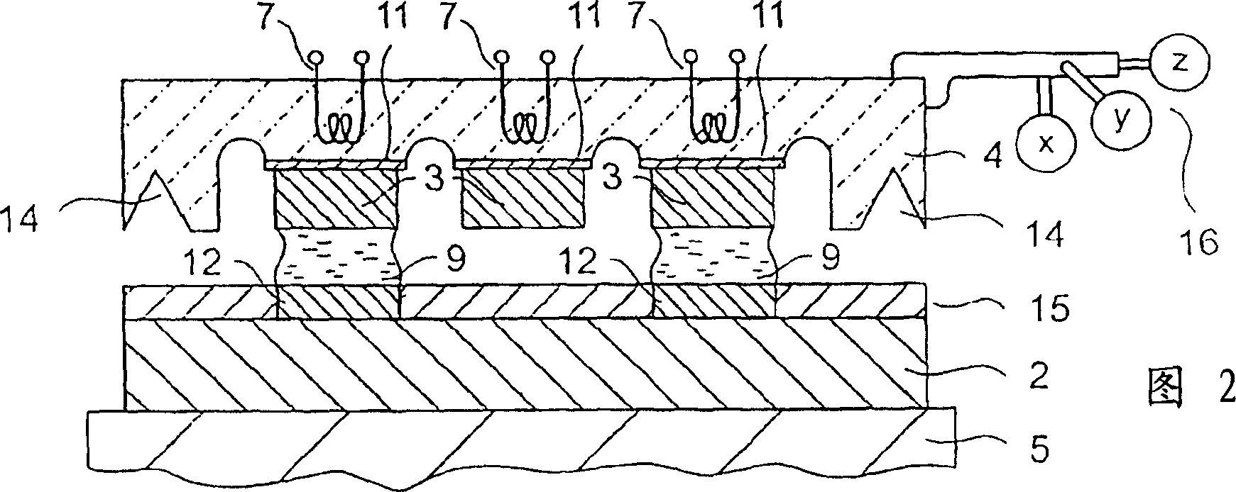
[0027] As shown in FIG. 2, a CMOS wafer 2 containing several chips is processed by any existing CMOS process. Therein, the process is stopped after the last metallization step. The chip has landing areas 12 for integrated circuit elements 3 (here VCSELs 3 ). The landing area 12 is now the signal pad for the desired optical input. Then, the entire CMOS wafer 2 is made hydrophobic except for the landing area 12 . It is thus covered with a wettability-structure layer 15 configured such that the landing zone 12 is hydrophilic and the rest of the wettability-structure layer 15 is hydrophobic. The CMOS wafer 2 is also referred to as the target substrate 2 representing the VCSELs 3 of the integrated circuit components 3 . The landing area 12 is a predetermined location 12 for these integrated circuit components 3 . The CMOS wafer 2 is fixed on the target substrate mount 5 .
[0028]As depicted ...
PUM
 Abstract
Description
Claims
Application Information


