Semiconductor device and its manufacturing method

A manufacturing method and semiconductor technology, which can be used in semiconductor/solid-state device manufacturing, semiconductor devices, semiconductor/solid-state device components, etc., and can solve problems such as low heat resistance

Inactive Publication Date: 2004-05-19
KK TOSHIBA
View PDF1 Cites 8 Cited by
  • Summary
  • Abstract
  • Description
  • Claims
  • Application Information

AI Technical Summary

Problems solved by technology

Other metals constituting silicides include Co, Mo, W, Ti, Ta, Hf, Pt, etc., but the heat resistance of any metal silicide is also low, for example, the heat resistance of Co silicide is 550°C , the heat resistance of the silicide of Mo is 650°C, and the heat resistance of the silicide of W is about 500°C or above

Method used


Image

  • Semiconductor device and its manufacturing method
  • Semiconductor device and its manufacturing method
  • Semiconductor device and its manufacturing method

Examples


Embodiment Construction

[0041] Embodiments of the present invention will be described below with reference to the drawings.

[0042] First refer to Figure 1 to Figure 6 The first embodiment will be described.

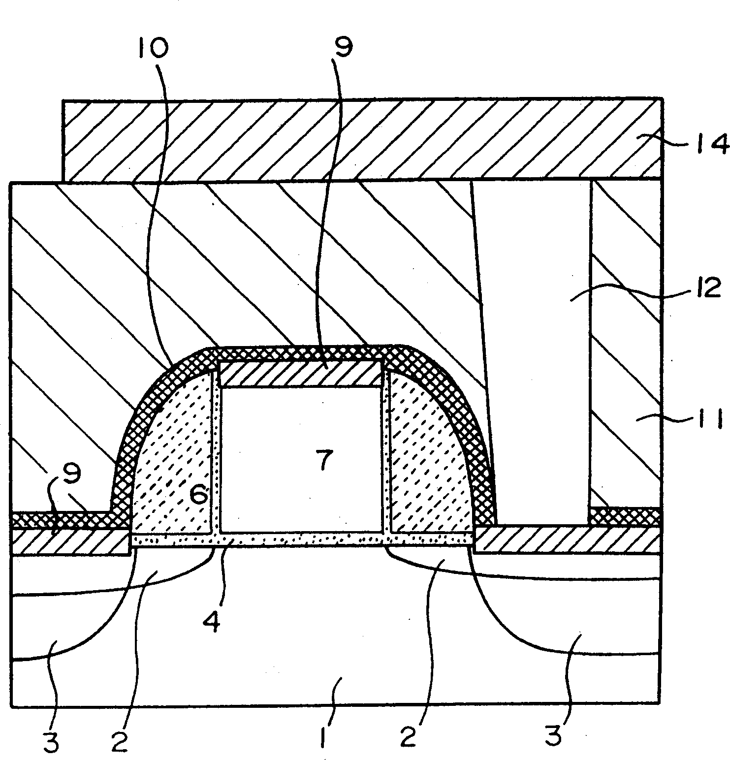
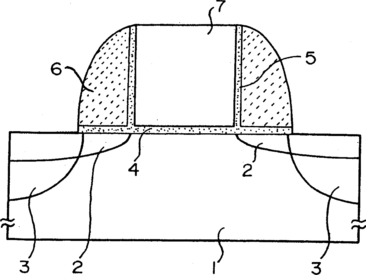
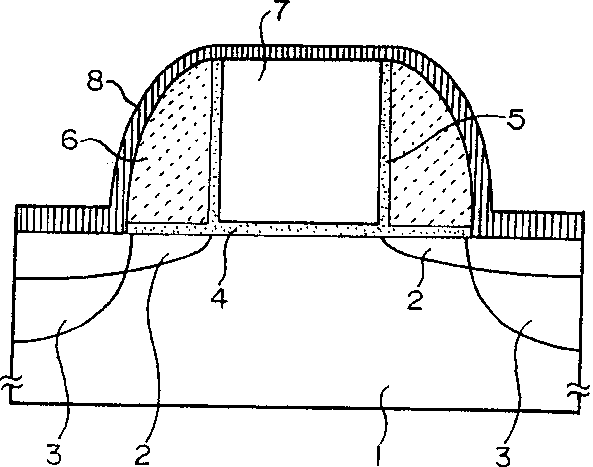
[0043] figure 1 is a cross-sectional view of a semiconductor device, Figure 2 to Figure 5 is a cross-sectional view of the manufacturing process of a semiconductor device, Image 6 is a characteristic diagram showing the results of SIMS analysis of impurities in a silicon nitride film (SiN) film formed by the method of this example.

[0044] The silicon semiconductor substrate 1 is, for example, P-type, and this figure is a cross-sectional view of the structure of an NMOSFET formed on the substrate. figure 1 The MOSFET shown in is used, for example, in a CMOS structure in which both NMOS and PMOS are formed within the same chip. and Figure 8 Likewise, on the semiconductor substrate 1, MOSFETs are formed in element regions divided by element isolation regions (not shown) such as STI. ...


PUM

PropertyMeasurementUnit
thermal resistanceaaaaaaaaaa

Abstract

A semiconductor device having an insulted silicon nitride layer insulated silicon nitride layer without deteriorating the metal silicide composed conduction layer and its manufacturing method are provided. Form an insulated film 10 mainly comprising uniform carbon-contented silicon nitride film on the metal silicide, for example, nickel silicide conduction layer 9. The carbon contented nitride film is made by reacting the nitrified seed and silicon source. Methyl-contented hexamethyldisilane is adopted as the silicon source, so the nitride film formed through the reaction consists of carbon and hydrogen. Furthermore, if it contains methyl, the film becomes porous, so the dielectric constant is reduced. Therefore, the RC delay-induced transistor speed degradation will be suppressed. By means of carbon-contented silicon nitride film, the metal silicide conduction layer is not deteriorated during process. The silicon source could be amino or free radical of amino having carbide.

Description

technical field [0001] The present invention relates to a semiconductor device using a silicon nitride film, and more particularly, to a semiconductor device that has a silicon nitride film that does not use metal silicide used as a conductive layer to achieve high performance, and a method for manufacturing the same. Deterioration of characteristics. Background technique [0002] In second-generation semiconductor devices, metal silicides such as nickel silicide are used to reduce electrode resistance. Figure 8 This is a cross-sectional view of a semiconductor device using a conventional metal silicide for conductive layers such as electrodes. The silicon semiconductor substrate 101 is, for example, P-type, and this figure is a cross-sectional view of the structure of an NMOSFET formed on the substrate. The MOSFET shown in the figure is used, for example, in a CMOS structure in which both NMOS and PMOS are formed in the same chip. [0003] On the semiconductor substrate ...

Claims


Application Information

Patent Timeline
Patent Type & Authority Applications(China)
IPC IPC(8): H01L21/28H01L21/318H01L21/3205H01L21/336H01L21/768H01L21/8234H01L21/8247H01L23/52H01L23/522H01L27/085H01L27/115H01L29/423H01L29/49H01L29/78H01L29/788H01L29/792
CPCH01L21/76834H01L21/76801H01L2924/0002H01L29/665H01L21/76828H01L21/3185H01L29/6659H01L29/6656H01L21/0217H01L2924/00
Inventor 田中正幸
Owner KK TOSHIBA
Why Eureka
Try Eureka