

Chemical mechanical polishing method and apparatus
A chemical-mechanical, grinding method technology, applied in grinding devices, grinding machine tools, abrasive surface conditioning devices, etc., which can solve problems such as difficulty in ensuring reliability, expansion, and reduction in copper wiring heights
- Summary
- Abstract
- Description
- Claims
- Application Information
AI Technical Summary
Problems solved by technology
Method used
Image

Examples
Embodiment approach 1
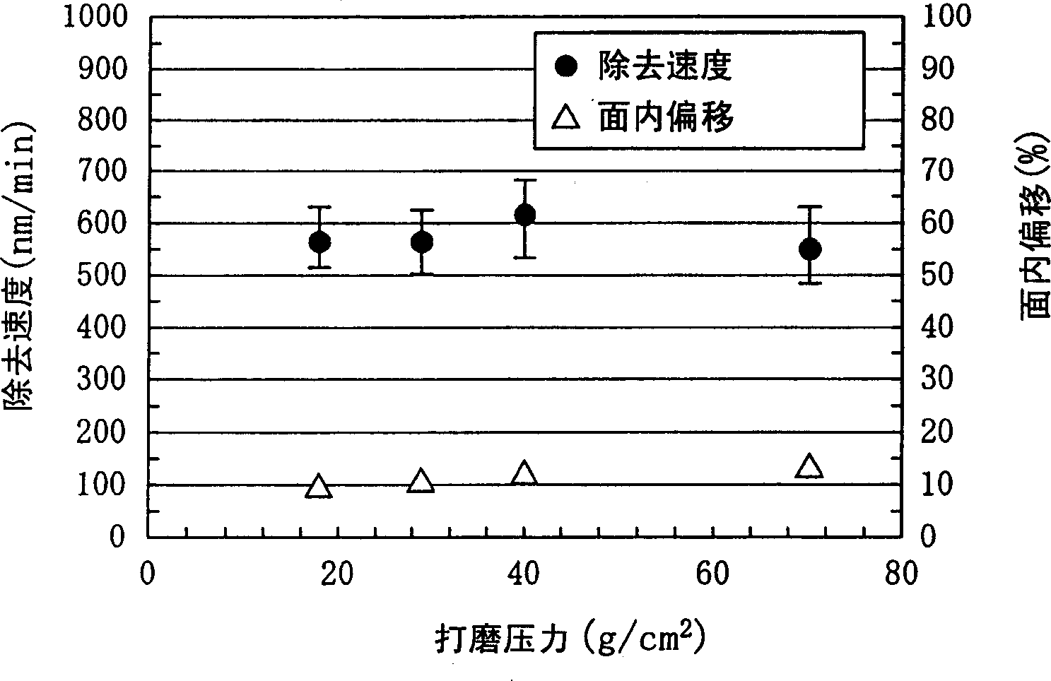
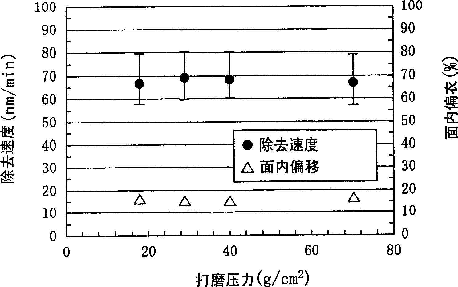
[0077] Next, an example of CMP using the optimum polishing conditions derived from the above-mentioned experimental results will be described. In addition, the entire process of forming embedded copper wiring including the CMP process is the same as Figure 8 (a)~(d), Figure 9 The methods described in (a) to (c) are the same, so the content of the CMP step will be described below.
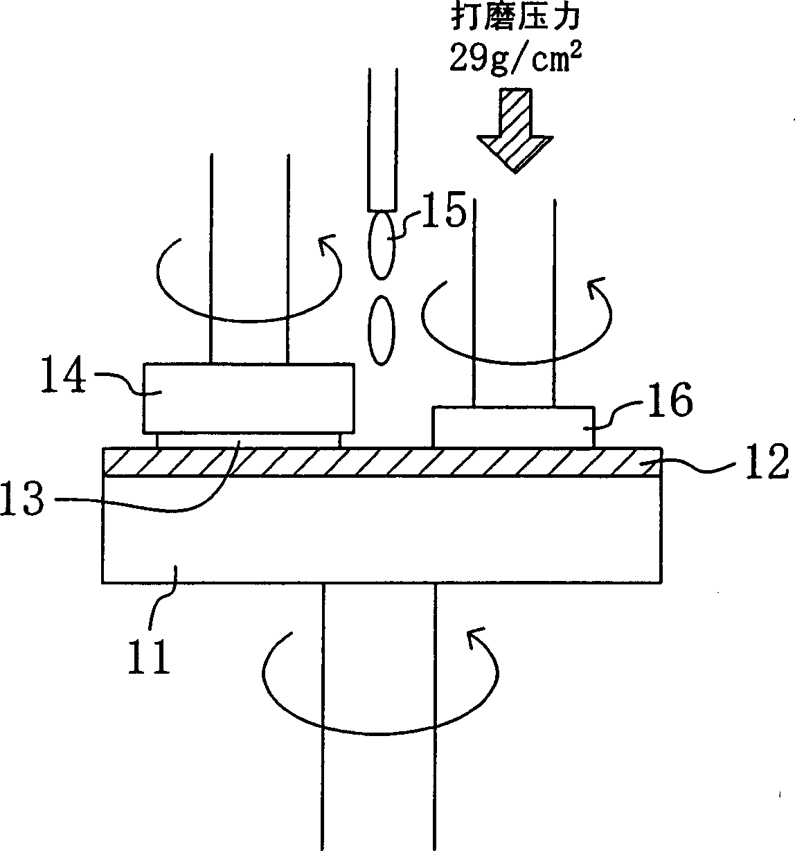
[0078] figure 1 is a diagram showing a schematic configuration of a chemical mechanical polishing apparatus used in the chemical mechanical polishing method according to Embodiment 1 of the present invention. Such as figure 1 As shown, the chemical mechanical polishing apparatus used in the chemical mechanical polishing method of this embodiment is the same as conventional ones.
[0079] That is, the chemical mechanical polishing apparatus used in the present embodiment includes: a polishing bottom plate 11 on which a polishing cloth 12 is installed; a holding table 14 having a rotating mecha...
Embodiment approach 2
[0089] Figure 5 It is a diagram showing a schematic configuration of a chemical mechanical polishing apparatus according to Embodiment 2 of the present invention. The chemical mechanical polishing apparatus of this embodiment is characterized in that the surface roughness of the polishing cloth is monitored before polishing or during polishing simultaneously with polishing. Next, it will be described in detail.
[0090] The chemical mechanical polishing apparatus used in this embodiment is the same as that used in Embodiment 1, and has: a polishing bottom plate 11 on which a polishing cloth 12 is installed; a holding table 14 for holding a substrate 13 to be polished; A sander 16 for roughening the upper surface of the abrasive cloth 12 . In addition, a torque measuring device 17 connected to a torque monitor 18 is attached to the polisher 16 of the chemical mechanical polishing apparatus of the present invention.
[0091] When the substrate 13 is polished, a load acts on ...
Embodiment approach 3
[0108] Figure 7 It is a diagram showing a schematic configuration of a chemical mechanical polishing apparatus according to Embodiment 3 of the present invention. The chemical mechanical polishing device of the present embodiment is characterized in that the distance between the polisher in a stationary state and the polishing cloth is always kept constant. A detailed description will be given below.
[0109] Such as Figure 7 As shown, the chemical mechanical polishing apparatus of the present embodiment is the same as the apparatus used in Embodiment 1, and has: a polishing bottom plate 11 on which a polishing cloth 12 is installed; a holding table 14 for holding a substrate 13 to be polished; A sander 16 for roughening the upper surface of the polishing cloth 12 . In addition, an electromagnetic wave transceiver 19 connected to the time measuring device 20 is attached to the sander 16 .
[0110] When the substrate 13 is polished, a load is applied to the holding table ...
PUM
| Property | Measurement | Unit |
|---|---|---|
| surface roughness | aaaaa | aaaaa |
| surface roughness | aaaaa | aaaaa |
Abstract
Description
Claims
Application Information