Transistor integrated circuit optimization method for process transplantation

A transistor-level, integrated circuit technology, applied in the field of integrated circuit optimization, can solve problems such as local optimum, without considering layout parasitic effects, etc., achieve fast optimization speed, optimize circuit performance, and avoid iteration effects

Inactive Publication Date: 2004-07-07
AIKESAILI MICROELECTRONICS TECH BEIJING
View PDF0 Cites 12 Cited by
  • Summary
  • Abstract
  • Description
  • Claims
  • Application Information

AI Technical Summary

Problems solved by technology

But this method of optimizing the circuit as a whole may lead to local optima instead of global optima
[0007] Although the circuit size is optimal, and the circuit simulation results also confirm that the circuit performanc

Method used


Image

  • Transistor integrated circuit optimization method for process transplantation
  • Transistor integrated circuit optimization method for process transplantation
  • Transistor integrated circuit optimization method for process transplantation

Examples


Example Embodiment

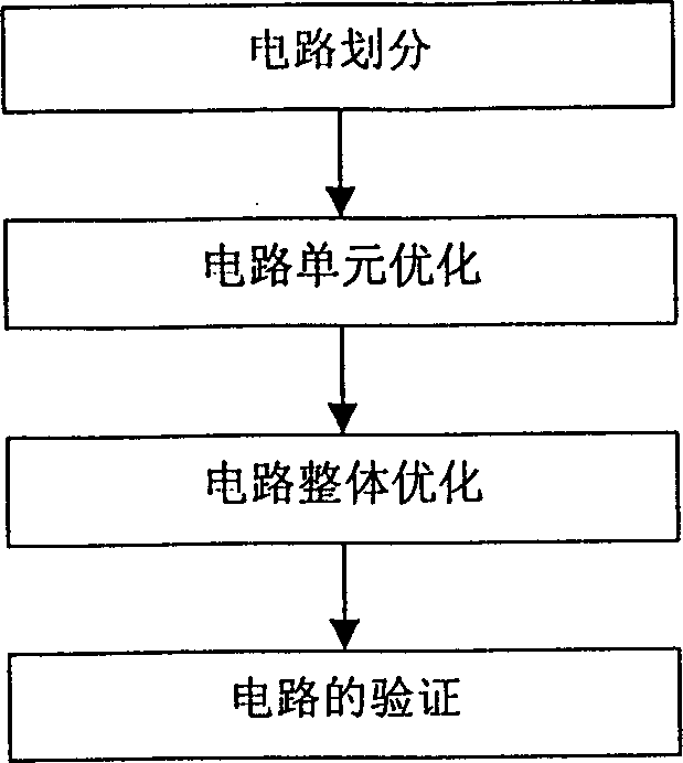
[0037] The present invention will be further described below with reference to the accompanying drawings and the following non-limiting examples.
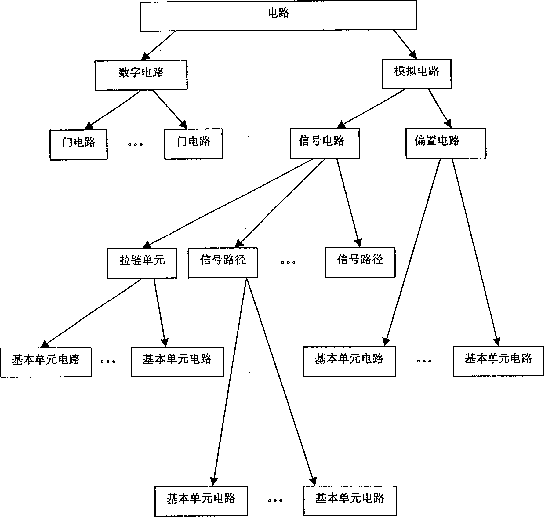
[0038] like figure 1 As shown, a transistor-level integrated circuit optimization technique for process migration, first divides the circuit into a digital circuit and an analog or radio frequency circuit: a complete circuit system usually includes a digital circuit subsystem and an analog or radio frequency circuit subsystem, because The characteristics of digital circuits are different from the operating characteristics of analog or radio frequency circuits. It is necessary to adopt different optimization methods for these two parts. Compared with the optimization of digital circuits, the optimization of analog or radio frequency circuits is more complicated. In order to better optimize The whole circuit, which has to divide them. The division method of transistor-level digital circuits and analog or radio frequency circuits ha...


PUM


Abstract

The present invention relates to a technique for optimizing automatically an integrated circuit of transistor stage designed with respect to one process to be another integrated circuit of transistor stage adapted to the other process. The object of the invention is to provide a software which can optimize automatically the physical dimension, the area and the property of the integrated circuit of transistor stage transplanted with respect to the process. The invention comprises the following steps: ( 1 ) dividing the circuit; ( 2 ) optimizing the circuit in unit; ( 3 ) optimizing the circuit in entirety; ( 4 ) verifying the circuit. The invention converts the optimization of a large circuit to the same of the limited kinds of basic unit circuits; optimizes the basic unit circuits using analytical method; accelerates the simulation of the circuit according to the result of the division thereof, shortening the time required for optimizing the circuit in entirety and analyzes the mismatch of the matching signal path, optimizing the key signal path.

Description

technical field [0001] The present invention relates to a transistor-level integrated circuit optimization technology oriented to process migration, more specifically, the present invention relates to automatically optimizing a transistor-level integrated circuit designed on one integrated circuit process to be suitable for another integrated circuit process The technical field of transistor-level integrated circuits. technical background [0002] When updating the process of integrated circuits, it is necessary to optimize the integrated circuits designed in the past to the integrated circuits under the new process conditions under the premise of ensuring the circuit performance indicators, so as to minimize the area. It includes two steps: transistor-level circuit transplantation and physical layout-level circuit transplantation. It is impossible to realize the physical layout optimization technology directly oriented to process migration. It must go through three steps: ...

Claims


Application Information

Patent Timeline
IPC IPC(8): H01L21/70H01L27/00
Inventor 张鹏飞张锡盛吴玉平
Owner AIKESAILI MICROELECTRONICS TECH BEIJING
Why Eureka
Try Eureka