

Semiconductor luminescent device and its manufacturing method
A technology for light-emitting devices and manufacturing methods, applied in semiconductor devices, electric solid-state devices, electrical components, etc., can solve problems such as affecting reliability, and achieve the effect of preventing the deterioration of processability and excellent thermal radiation performance.
- Summary
- Abstract
- Description
- Claims
- Application Information
AI Technical Summary
Problems solved by technology
Method used
Image

Examples
no. 1 example
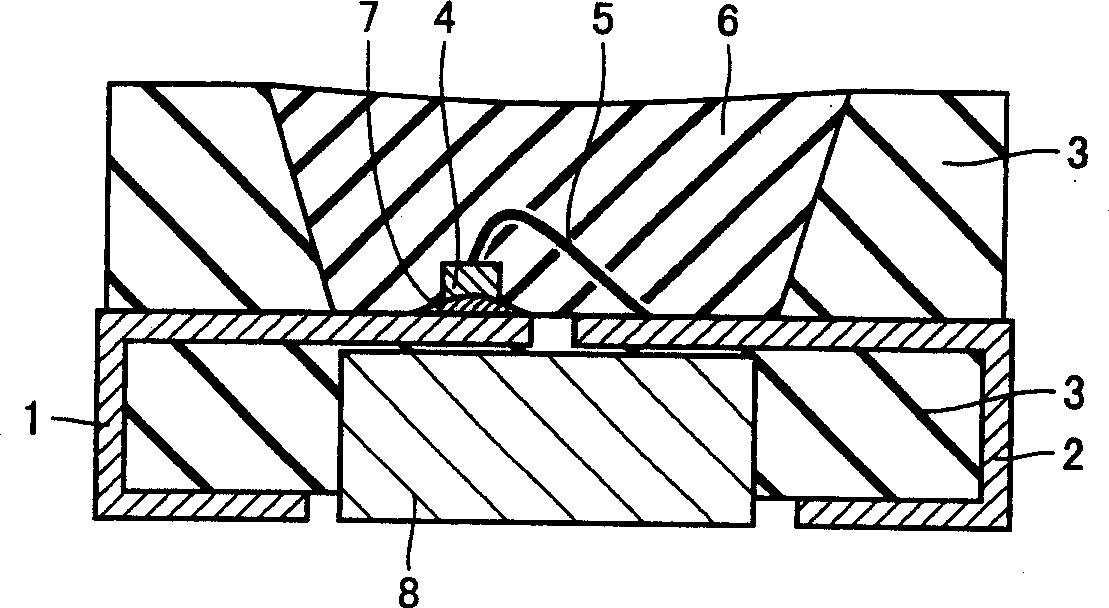
[0037] figure 1 It is a cross-sectional view of the surface-mounted LED according to the first embodiment of the present invention.
[0038] The semiconductor light emitting device of the first embodiment includes: an LED chip 4; a first lead frame 1 on which the LED chip 4 is mounted; and a second lead frame 2 which is electrically connected to the LED chip by a bonding wire 5 such as a gold wire 4; Resin part 3, which surrounds the LED chip 4 and fixes the lead frame. The metal body 8 is located under the area where the LED chip 4 is mounted on the first lead frame 1.
[0039] The first lead frame 1 and the second lead frame 2 are embedded in the resin part 3 by insert molding. The LED chip 4 is mounted on the first lead frame 1 with the Ag paste 7 in between. The bonding wire 5 is connected to the second lead frame 2. Therefore, the second lead frame 2 is mechanically and electrically connected to the LED chip 4. The resin portion 3 is formed to surround the periphery of the LE...
no. 2 example
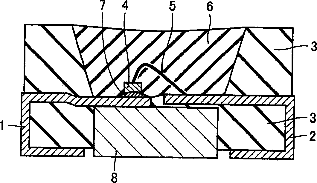
[0049] figure 2 It is a cross-sectional view of a surface-mounted LED according to the second embodiment of the present invention.
[0050] The semiconductor light emitting device of the second embodiment is an improvement of the semiconductor light emitting device of the first embodiment. The metal body 8 is in contact with the first lead frame 1.
[0051] For example, the first lead frame 1 mounted with the LED chip 4 is set lower than the second lead frame 2 so that contact with the metal body 8 is established. in figure 2 In the example shown, the first lead frame 1 is bent to form contact with the metal body 8.
[0052] Therefore, the heat generated by the LED chip 4 is sequentially transferred through the first lead frame 1, the metal body 8, and the mounting board. There is no gap between the first lead frame 1 and the metal body 8 in the first embodiment, so that the heat generated at the LED chip 4 is more effectively transferred to the mounting board. Although the fir...
no. 3 example
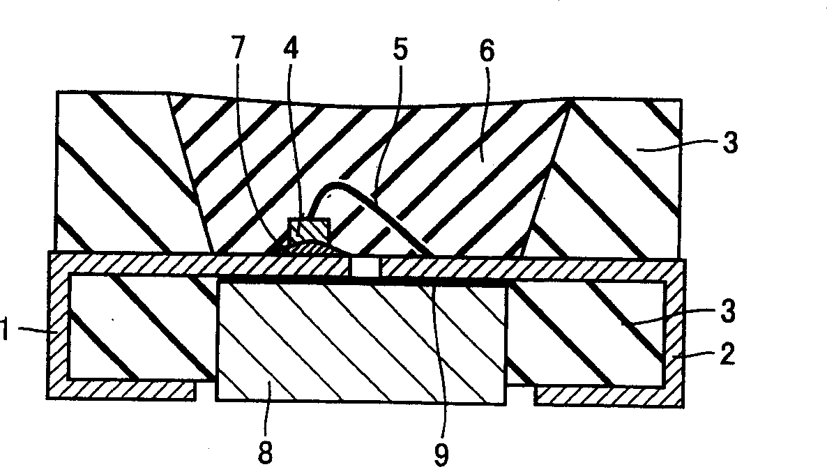
[0055] image 3 It is a cross-sectional view of a surface-mounted LED according to the third embodiment of the present invention.
[0056] The semiconductor light emitting device of the third embodiment is another improvement of the semiconductor light emitting device of the first embodiment. On the surface of the metal body 8 is provided an electrical insulation treatment portion 9 formed, for example, by applying an insulating film, an insulating coating, or by anodizing. The surface of the insulating metal body 8 is in contact with the first lead frame 1 and the second lead frame 2.
[0057] In the semiconductor light emitting device of the second embodiment, whether a single LED chip or multiple LED chips are used, as long as the LED chips are located on the same lead frame, the heat generated by the LED chip 4 can be transferred to the mounting board, and the first lead There is no part corresponding to the gap in the first embodiment between the frame 1 and the metal body 8...
PUM
 Abstract
Description
Claims
Application Information