Method of mfg. semiconductor device

A manufacturing method and semiconductor technology, applied in semiconductor/solid-state device manufacturing, electrical components, circuits, etc., can solve the problems of rising manufacturing cost, complicated manufacturing process, and high manufacturing unit price

Inactive Publication Date: 2004-08-11
SANYO ELECTRIC CO LTD
View PDF1 Cites 2 Cited by
  • Summary
  • Abstract
  • Description
  • Claims
  • Application Information

AI Technical Summary

Problems solved by technology

[0013] But when Figure 17 ~ Figure 27 In the shown conventional semiconductor manufacturing device including the element isolation region, since the redundant deposition part of the HDP-NSG film 107 buried in the shallow trench 120 and the redundant deposition part of the silicon oxide film 111 buried in the deep trench 130 are respectively formed by There is a problem that the manufacturing process is complicated because it is removed by grinding in a different CMP process
Furthermore, since it is necessary to form Si as a stopper film in each CMP process, 3 N 4 Membrane 105 and Si 3 N 4 film 108, which also has the problem of complicating the manufacturing process
Furthermore, since the manufacturing unit price of the CMP process is high, the CMP process is performed twice, and there is a problem of increasing the manufacturing cost.

Method used


Image

  • Method of mfg. semiconductor device
  • Method of mfg. semiconductor device
  • Method of mfg. semiconductor device

Examples


Embodiment Construction

[0036] Specific embodiments of the present invention will be described below based on the drawings.

[0037] Refer to the following Figure 1 to Figure 11 The manufacturing process of the semiconductor device including the element isolation region of this embodiment will be described.

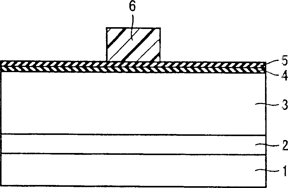
[0038] First, if figure 1 As shown, on the P-type silicon substrate 1, N + Type buried layer 2. in N + On the N-type buried layer 2, an N-type epitaxial silicon layer 3 is formed. Also, the P-type silicon substrate 1, N + The N-type buried layer 2 and the N-type epitaxial silicon layer 3 are examples of the "semiconductor substrate" of the present invention. Furthermore, on the N-type epitaxial silicon layer 3, a silicon oxide film (SiO 2 film) 4. On the silicon oxide film 4, a Si with a thickness of about 100 nm is formed as a stopper film by a CMP process. 3 N 4 Film 5. Moreover, in Si 3 N 4 A resist film 6 is formed in a predetermined area of ​​the film 5 .

[0039] Next, if ...


PUM


Abstract

A method of fabricating a semiconductor device capable of suppressing defective etching in formation of a deep trench also when the number of polishing steps is reduced is obtained. This method of fabricating a semiconductor device comprises steps of forming a first trench on an element isolation region of a semiconductor substrate, forming a first film consisting of an insulator film to fill up the first trench, forming a second trench larger in depth than the first trench in the first trench, forming an embedded film in the second trench and substantially simultaneously polishing an excess depositional portion of the first film and an excess depositional portion of the embedded film.

Description

technical field [0001] The present invention relates to a method of manufacturing a semiconductor device, and more particularly to a method of manufacturing a semiconductor device having an element isolation region. Background technique [0002] Conventionally, as an element isolation technology for semiconductor devices such as bipolar transistors, it is known to use a field oxide film formed by the LOCOS (Local Oxidation of Silicon) method to perform element isolation, and to form an element for isolation. A deep trench method for a high-concentration impurity layer in a substrate. In the field oxide film formed by such a LOCOS method, the flatness of the surface is poor, and the area of ​​the element isolation region is increased due to the sharp tip, which makes further miniaturization difficult. [0003] Therefore, in recent years, instead of the LOCOS method, an element isolation technology using an STI (shallow trench isolation) method, which is excellent in flatness...

Claims


Application Information

Patent Timeline
Patent Type & Authority Applications(China)
IPC IPC(8): H01L21/308H01L21/762H01L21/8234
CPCH01L21/3081H01L21/823481H01L21/76232
Inventor 井原良和
Owner SANYO ELECTRIC CO LTD
Why Eureka
Try Eureka