Defect detecting parametric analysis method

A defect detection and parameter analysis technology, which is applied in semiconductor/solid-state device testing/measurement, electrical components, semiconductor/solid-state device manufacturing, etc., can solve problems such as limited ability of engineers, increased production cost, frequent replacement, etc., to improve online production Situation, reduce production cost, improve the effect of yield rate

Inactive Publication Date: 2004-08-18
POWERCHIP SEMICON CORP
View PDF0 Cites 19 Cited by
  • Summary
  • Abstract
  • Description
  • Claims
  • Application Information

AI Technical Summary

Problems solved by technology

[0008] However, since the existing technology uses human experience judgment to determine the analysis results (step 103), the accuracy and credibility of the final analysis results will be questionable; The experience among engineers is not easy to pass on, and each engineer has limited ability and cannot take into account the operating status of all machines in the factory. Therefore, when the defect detection results of semiconductor products are abnormal, the engineers may not have enough experience to quickly and correctly It may take a lot of time to conduct relevant research to determine which link has a problem, and it may even make a wrong judgment. In this way, not only will the efficiency of the manufacturing process be reduced, the production cost will be increased, and the production situation will not be improved in time. Improve yield

Method used


Image

  • Defect detecting parametric analysis method
  • Defect detecting parametric analysis method
  • Defect detecting parametric analysis method

Examples


Embodiment Construction

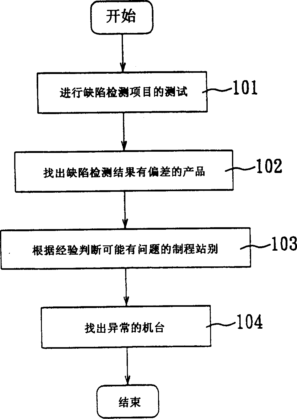
[0030] The defect detection parameter analysis method according to the preferred embodiment of the present invention will be described below with reference to the accompanying drawings, wherein the same components are represented by the same symbols.

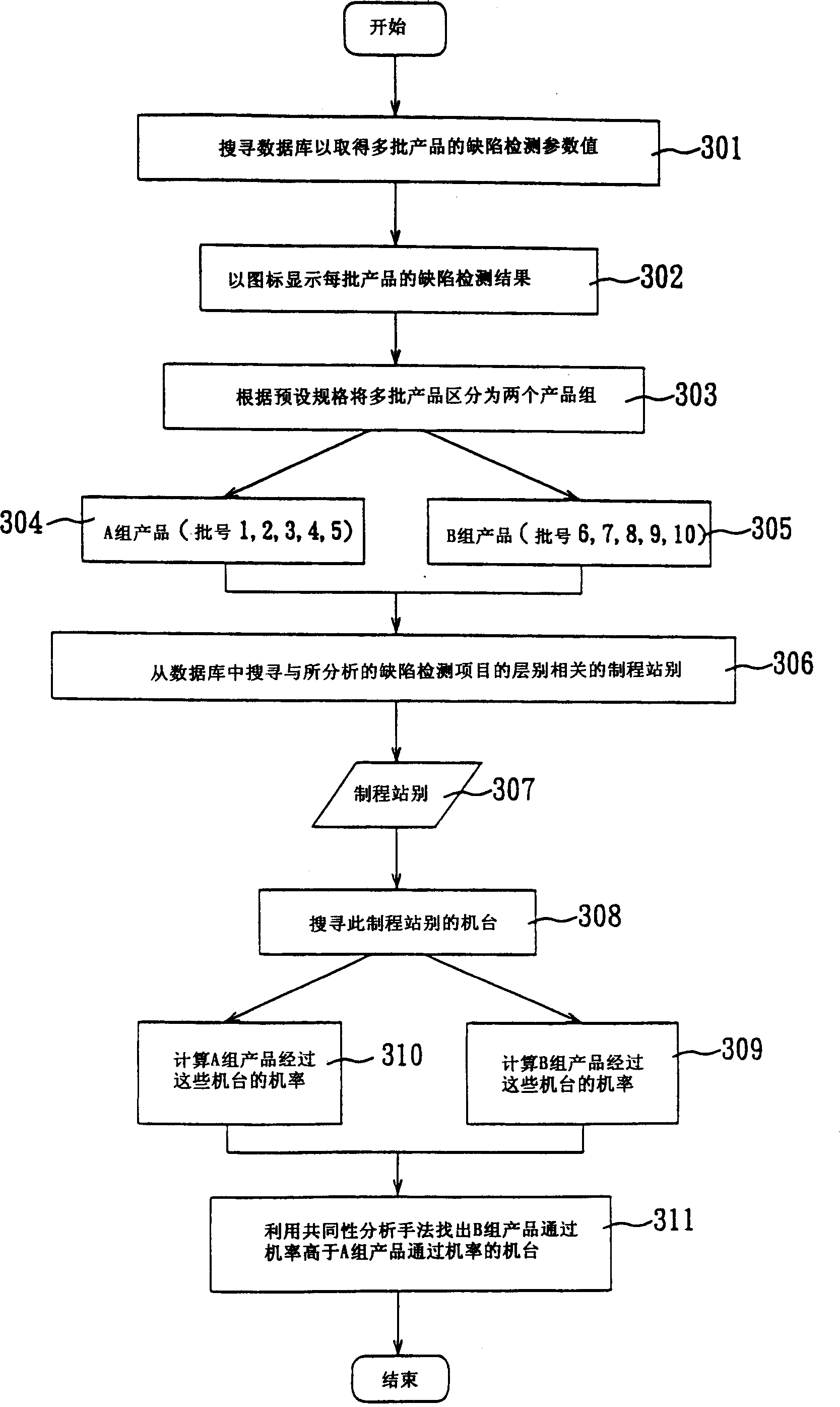
[0031] Such as image 3 As shown, the figure shows the flow chart of the defect detection parameter analysis method of the preferred embodiment of the present invention, which is used to quickly and correctly determine which machine has a problem when the defect detection data of a semiconductor product is abnormal.

[0032] First, step 301 searches a database to obtain defect detection parameter values ​​of multiple batches of products. Among them, each batch (lot) of products has a lot number (lot number), and each batch of products includes 25 wafers, and each batch of products passes through multiple machines with multiple processes, and one or more wafers in each batch of products of the wafers are inspected by at least on...


PUM


Abstract

A defect detecting parametric analysis method comprises the steps of, searching the data base to obtain the defect detecting parameter value for a plurality of products, dividing the products into at least one acceptable product group and one disqualified product group, searching the process stations relating to the defect detecting items from the data base, searching for machine benches where the acceptable product set passes during the process, searching for machine benches where the disqualified product set passes during the process, determining the machine bench in which the passing probability of the disqualified product set is higher than that of the acceptable product set.

Description

technical field [0001] The invention relates to a process parameter analysis method, in particular to a defect detection parameter analysis method. Background technique [0002] In semiconductor manufacturing technology, to complete a semiconductor product, it usually has to go through many processes, such as lithography process, etching process, ion implantation process, etc.; that is to say, a large number of machines must be applied in the semiconductor manufacturing process, and Many cumbersome procedures. Therefore, those who are familiar with this technology are committed to ensuring the normal operation of the machine, maintaining or improving product yield, detecting and confirming problems, and machine maintenance, so as to make the production speed and quality of semiconductor products meet customer needs. [0003] Generally speaking, in order to discuss the problems of semiconductor manufacturing process, the analysis can be started from the following data, inclu...

Claims


Application Information

Patent Timeline
Patent Type & Authority Applications(China)
IPC IPC(8): H01L21/00H01L21/66
Inventor 戴鸿恩罗皓觉
Owner POWERCHIP SEMICON CORP
Why Eureka
Try Eureka