Information processor and memory access arranging method

An information processing device and memory technology, applied in memory systems, electrical digital data processing, instruments, etc., can solve the problems of external access speed reduction and final set operation speed reduction, etc.

Inactive Publication Date: 2004-09-22
PANASONIC CORP
View PDF0 Cites 7 Cited by
  • Summary
  • Abstract
  • Description
  • Claims
  • Application Information

AI Technical Summary

Problems solved by technology

In the case of applying this mechanism to transfer data from an external processor to a memory provided in the processor through an external input / output mechanism, the external access speed is thereby reduced, and in addition, the operation speed of the final set is also reduced

Method used


Image

  • Information processor and memory access arranging method
  • Information processor and memory access arranging method
  • Information processor and memory access arranging method

Examples


no. 1 example

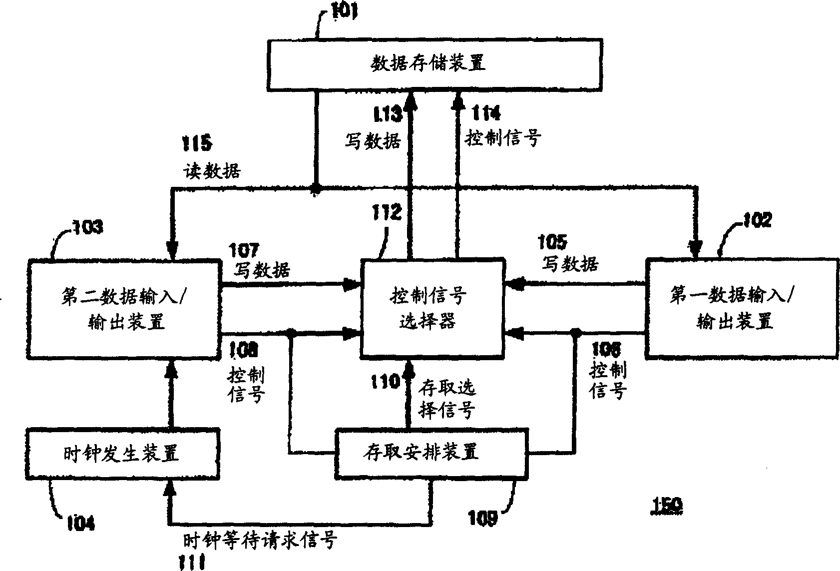
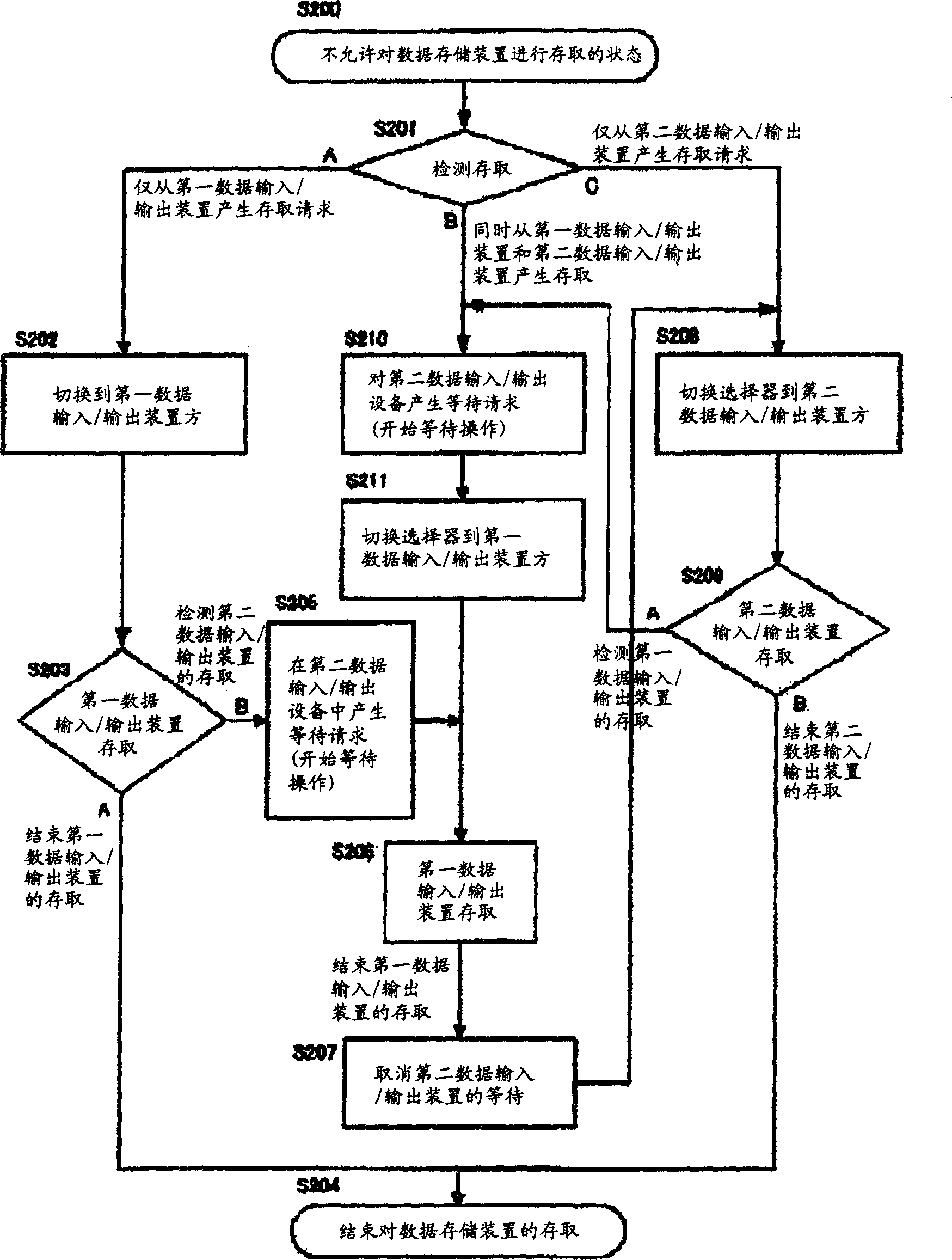
[0032] attached figure 1 is a block diagram showing the structure of an information processing apparatus according to a first embodiment of the present invention. in the attached figure 1 , the information processing device 150 includes a data storage device 101, a first data input / output device 102, which has a high access priority to the data storage device 101, and a second data input / output device 103, which has a low access priority, The clock generating means 104 is used to provide a clock to the second data input / output means 103 , the access arrangement means 109 , and the control signal selector 112 .

[0033] The access arrangement device 109 monitors the control signal 106 of the first data input / output device 102 and the control signal 108 of the second data input / output device 103, and generates an access selection signal 110 for use in the first data input / output device Switching between 102 and the second data input / output device 103 will provide both control ...

no. 2 example

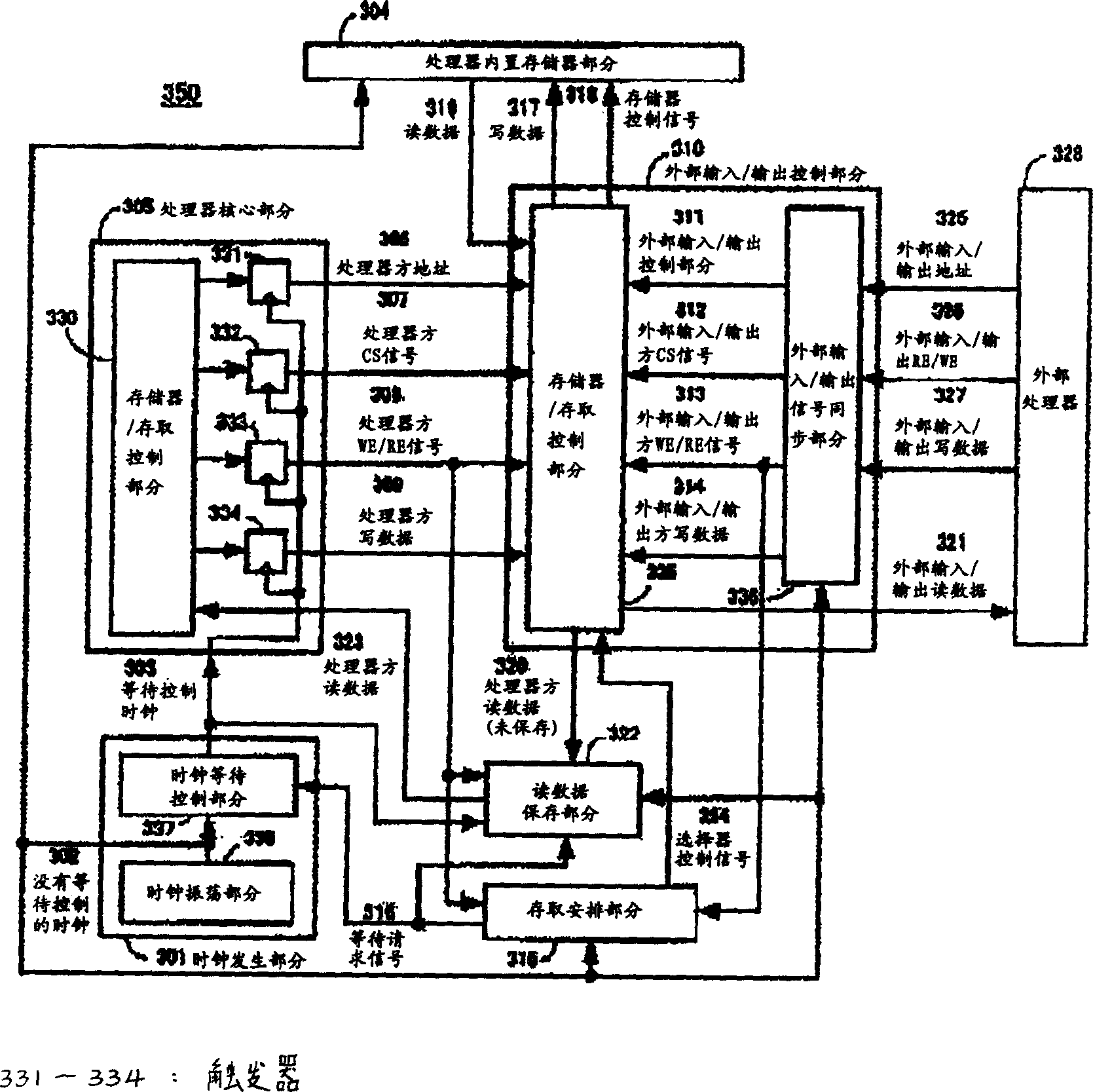
[0042] attached image 3 is a block diagram showing a schematic configuration of an information processing apparatus according to a second embodiment of the present invention. in the attached image 3 , an information processing apparatus 350 includes a clock generation section 301, a processor built-in memory section 304 provided in the processor and accessible from outside the processor, a processor core section 305 for performing pipeline processing by instructions, an external input The / output control section 310, which has a higher access priority than the access priority of the processor core section 305 to the processor built-in memory 304, reads the data storage section 322 for saving the output from the external input / output control section 310 The processor side read data 320 and the access scheduling part 315 are used to generate the wait request signal 316 when the processor core part 305 and the external input / output control part 310 access simultaneously.

[0...


PUM


Abstract

It is an object to implement a small-scale data input / output mechanism to a memory at a high speed with a priority all the time for a memory provided in a processor. In an information processing apparatus including a processor for carrying out a pipeline processing over an instruction, a memory provided in the processor and input / output control means for giving access to the memory with a high priority, a memory access arranging method includes a step (S512) of causing a clock to be supplied to the processor to wait when a contention of access of the processor and the input / output control means to the memory is generated, a step (S506) of executing the access of the input / output control means to the memory, and a step (S507, S511) of canceling the clock wait of the processor after ending the access of the input / output control means to the memory, and executing the access of the processor to the memory.

Description

technical field [0001] The present invention relates to an information processing device including an external input / output mechanism that can perform high-speed reading or writing between a memory device provided in a processor and an external device, and a A method of memory access scheduling in case of access contention to a memory device. Background technique [0002] Typically, dual-port memory is used as the easiest method of implementation when multiple control devices are performing reads from or writes to one memory device. However, in recent years, emphasis has been placed on system LSIs in the LSI market, and the scale of circuits has increased. For this reason, a dual-port memory occupying a large-area chip in a system LSI that requires a large-capacity memory is disadvantageous in terms of cost. Therefore, in order to reduce the chip area, it may be suggested to use a single-port memory. However, based on the timing of multiple control device accesses, access...

Claims


Application Information

Patent Timeline
Patent Type & Authority Applications(China)
IPC IPC(8): G06F12/00G06F13/14G06F13/16G06F13/20G06F13/362G06F13/42
CPCG06F13/161G06F13/1689
Inventor 森敦弘
Owner PANASONIC CORP
Why Eureka
Try Eureka