Semiconductor memory card, semiconductor memory control apparatus, and semiconductor memory control method

a technology of semiconductor memory and control apparatus, which is applied in the direction of memory adressing/allocation/relocation, instruments, sustainable buildings, etc., can solve the problems of reducing the free block, consuming a lot of time until writing completely, and wasting a lot of time erasing, etc., to achieve the effect of increasing the free block without lowering the processing performan

Active Publication Date: 2010-02-02
PANASONIC CORP
View PDF12 Cites 25 Cited by
  • Summary
  • Abstract
  • Description
  • Claims
  • Application Information

AI Technical Summary

Benefits of technology

[0009]According to the present invention, the number of erase blocks is determined based on a write start address and a write size obtained from the access unit, and the erase block is erased in accordance with data writing. Consequently, erasing can be performed without exposing the erase time and without lowering the processing performance, and a free block can be increased. A high-speed access to a semiconductor memory card, therefore, can be realized.

Problems solved by technology

There has been a problem in that the file system needs to perform a two-stage operation in which data is first erased in rewriting data and thereafter data is written, resulting in much time consumed until finishing writing completely.
Accordingly, there has been a drawback in that it takes lots of time to perform erasing in the case of a small data size and, therefore, the entire writing time becomes longer after all.

Method used


Image

  • Semiconductor memory card, semiconductor memory control apparatus, and semiconductor memory control method
  • Semiconductor memory card, semiconductor memory control apparatus, and semiconductor memory control method
  • Semiconductor memory card, semiconductor memory control apparatus, and semiconductor memory control method

Examples


embodiment 1

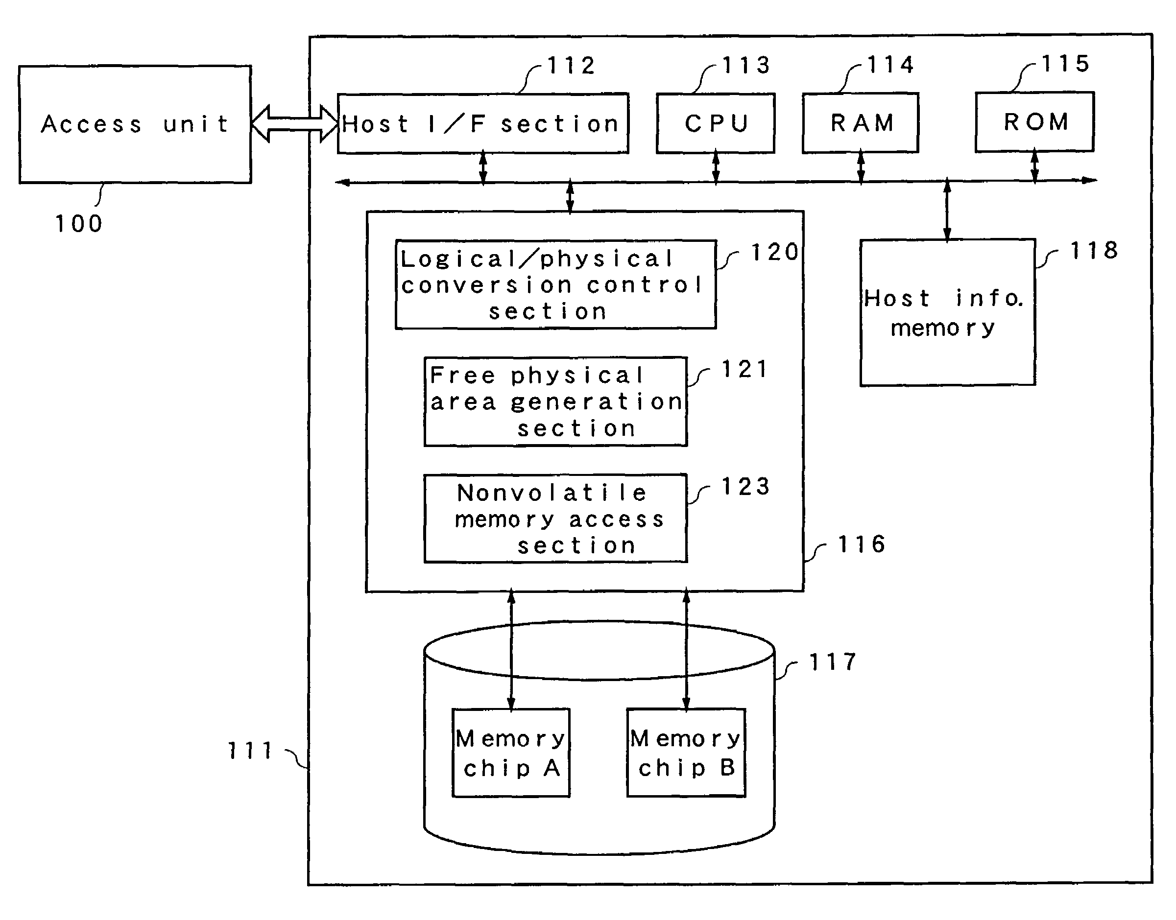
[0031]FIG. 1 is a block diagram showing a semiconductor memory card and an access unit according to Embodiment 1 of the present invention. In FIG. 1, an access unit 100 is connected to a semiconductor memory card 111. The semiconductor memory card 111 includes a host interface (I / F) section 112, a CPU 113, a RAM 114, a ROM 115, a memory controller 116, a nonvolatile memory 117, and a host information memory 118. The host interface section 112 is an interface for sending / receiving control signals and data to / from the access unit 100. The ROM 115 stores a program for controlling the semiconductor memory card 111. The program runs on the CPU 113 using the RAM 114 as a temporary storage area. The memory controller 116 is an element for controlling the nonvolatile memory 117. The nonvolatile memory 117 is a data storage area in the semiconductor memory card 111. The memory controller 116 includes a logical / physical conversion control section 120, a free physical area generation section 1...

embodiment 2

[0049]FIG. 9 is a block diagram showing a semiconductor memory card according to Embodiment 2 of the present invention. In this figure, an access unit 100 is connected to a semiconductor memory card 111. The semiconductor memory card 111 includes a host interface (I / F) section 112, a CPU 113, a RAM 114, a ROM 115, a memory controller 141, a nonvolatile memory 117, and a host information memory 142. The host interface section 112 is an interface for sending / receiving control signals and data to / from the access unit 100. The ROM 115 stores a program for controlling the semiconductor memory card 111. The program runs on the CPU 113 using the RAM 114 as a temporary storage area. The memory controller 116 is an element for controlling the nonvolatile memory 117. The nonvolatile memory 117 is a data storage area in the semiconductor memory card 111. The memory controller 141 includes a logical / physical conversion control section 143 and a nonvolatile memory access section 144. The logical...

embodiment 3

[0067]Next, Embodiment 3 of the present invention will be described. FIG. 13 is a block diagram showing a semiconductor memory card according to this embodiment. In FIG. 13, an access unit 100 is connected to a semiconductor memory card 111. The semiconductor memory card 111 includes a host interface (I / F) section 112, a CPU 113, a RAM 114, a ROM 115, a memory controller 151, a nonvolatile memory 117, and a host information memory 155. The host interface section 112 is an interface for sending / receiving control signals and data to / from the access unit 100. The ROM 115 stores a program for controlling the semiconductor memory card 111. The program runs on the CPU 113 using the RAM 114 as a temporary storage area. The memory controller 151 is an element for controlling the nonvolatile memory 117. The nonvolatile memory 117 is a data storage area in the semiconductor memory card 111. The memory controller 151 includes a logical / physical conversion control section 152, a free physical a...


PUM


Abstract

A host information memory is provided in a semiconductor memory card and a data write start address and a data size supplied by an access unit are stored. A free physical area generation section determines whether or not to perform erasing of an invalid block of a nonvolatile memory when writing of data based on the data write start address and data size, and determines the number of blocks to be erased. When erasing, writing of data and erasing of invalid blocks are simultaneously performed with respect to different memory chips. Erase process of data, herewith, can be optimized and high speed access from the access unit to a semiconductor memory card can be realized.

Description

TECHNICAL FIELD[0001]The present invention relates to a semiconductor memory card, a semiconductor memory control apparatus, and a semiconductor memory control method.BACKGROUND ART[0002]Various kinds of recording media for recording digital data such as music contents and visual data are there, such as magnetic disks, optical disks, and magnetic optical disks. A semiconductor memory card, which is one type of such recording media, uses a semiconductor memory such as a flash ROM (Read Only Memory) as a recording element and makes it possible to reduce a size of a recording medium; therefore, semiconductor memory card is rapidly spreading with a focus on small size mobile apparatuses, such as digital still cameras and mobile telephone terminals.[0003]Since data stored in a semiconductor memory card are managed by a file system, users can easily treat the stored data as a file. There is a FAT file system, used as a conventional file system, disclosed in ISO / IEC9293, “Information Techn...

Claims


Application Information

Patent Timeline
Patent Type & Authority Patents(United States)
IPC IPC(8): G06F12/00G06F3/06G06F3/08G06F12/02G06F12/06G06K17/00
CPCG06F3/0611G06F3/0625G06F3/0658G06F3/0688G06F12/0246G06F3/0659Y02B60/1246Y02D10/00
Inventor MAEDA, TAKUJIINOUE, SHINJIGOTOH, YOSHIHOOHARA, JUNNAKANISHI, MASAHIROTSUJITA, SHOICHIIZUMI, TOMOAKIKASAHARA, TETSUSHITAMURA, KAZUAKIMATSUNO, KIMINORIHORIUCHI, KOICHIINOUE, MANABU
Owner PANASONIC CORP
Why Eureka
Try Eureka