Molecular memory medium and molecular memory integrated circuit

a molecular memory and integrated circuit technology, applied in special recording techniques, instruments, nuclear engineering, etc., can solve the problems of difficult or impossible building structures using existing tools, current atom and molecule movement technologies are not practical, etc., and achieve high speed access to information stored and a large range of effects

Inactive Publication Date: 2007-08-21
NANOCHIP
View PDF203 Cites 23 Cited by
  • Summary
  • Abstract
  • Description
  • Claims
  • Application Information

AI Technical Summary

Benefits of technology

[0033]7) The present invention utilizes platforms of very low mass. As a result, the present invention provides fast access speed.
[0043]e) analyzing patterns of current and / or voltage between a fine tip and the surface of the molecular media which vary over time during the reading of each bit, in conjunction with topological information concerning the media surface computed dynamically, to provide very high speed access to the information stored.
[0045]The medium of a molecular memory surface can be any one of a large class of materials. The present invention describes a number of different materials, and several different techniques for reading and writing the materials. The present invention allows for a large class of materials to be used as the memory surface by virtue of the ability of the read / write head to fly above a relatively uneven surface at very high speeds, and the large range of forces with which to read and write information.

Problems solved by technology

Current technologies using movement of atoms and molecules (molecular scale technologies) are not practical because my problems exist regarding the efficient reading, writing (including maintaining a high density of storage) on media materials.
Further problems with current devices include structures that are difficult or impossible to build using existing tools.

Method used


Image

  • Molecular memory medium and molecular memory integrated circuit
  • Molecular memory medium and molecular memory integrated circuit
  • Molecular memory medium and molecular memory integrated circuit

Examples


Embodiment Construction

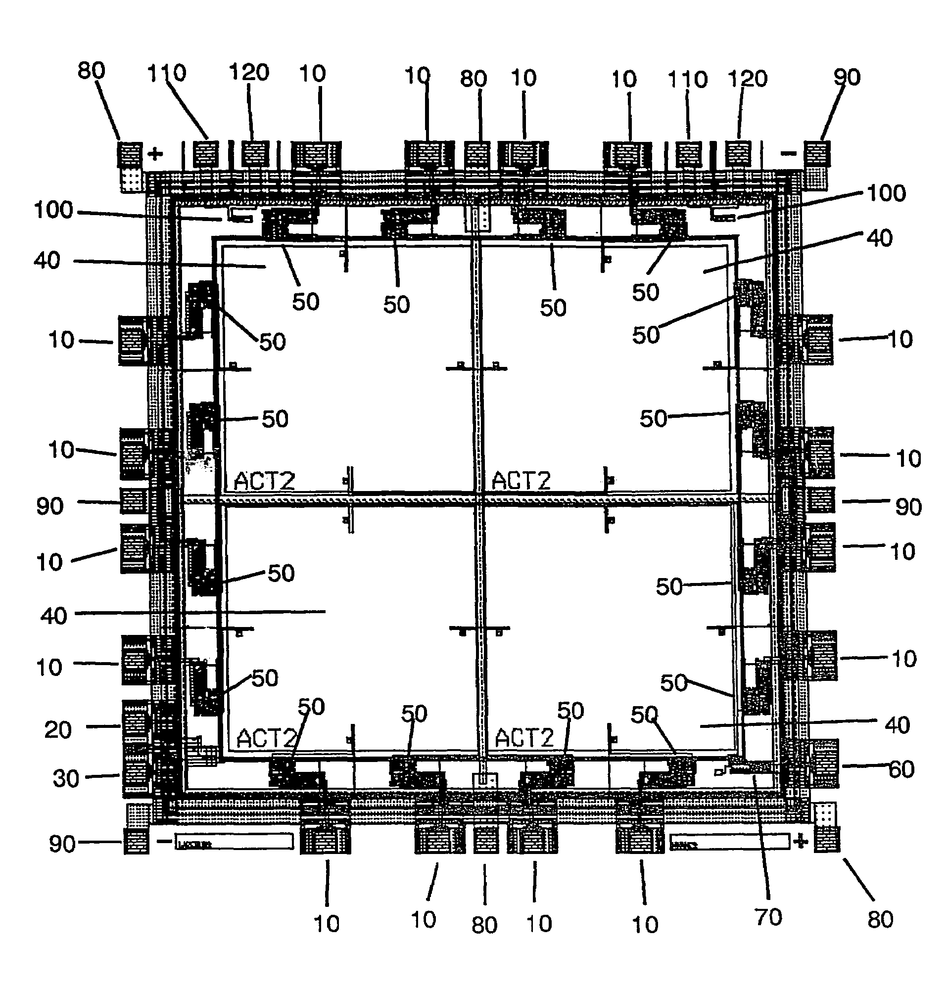
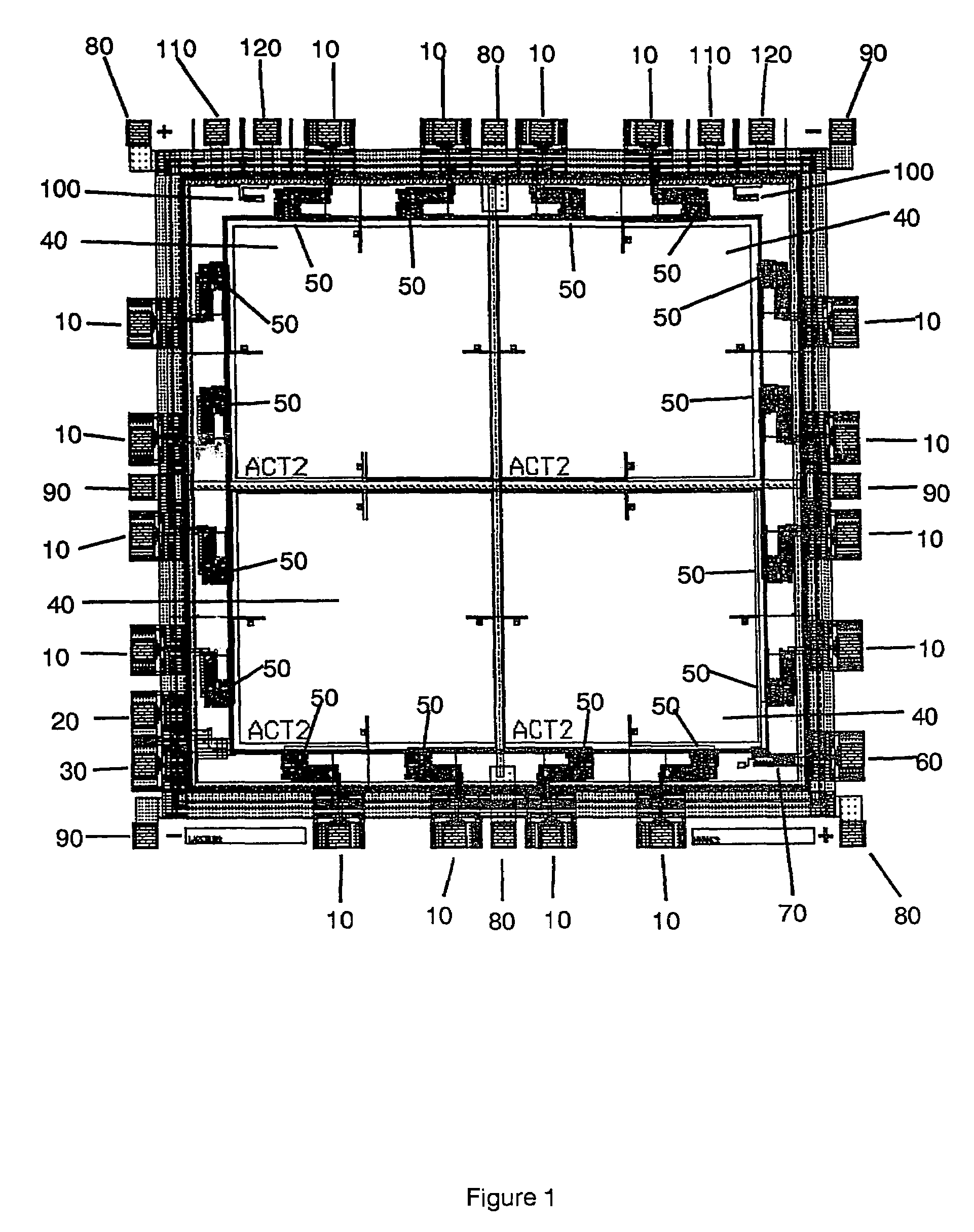
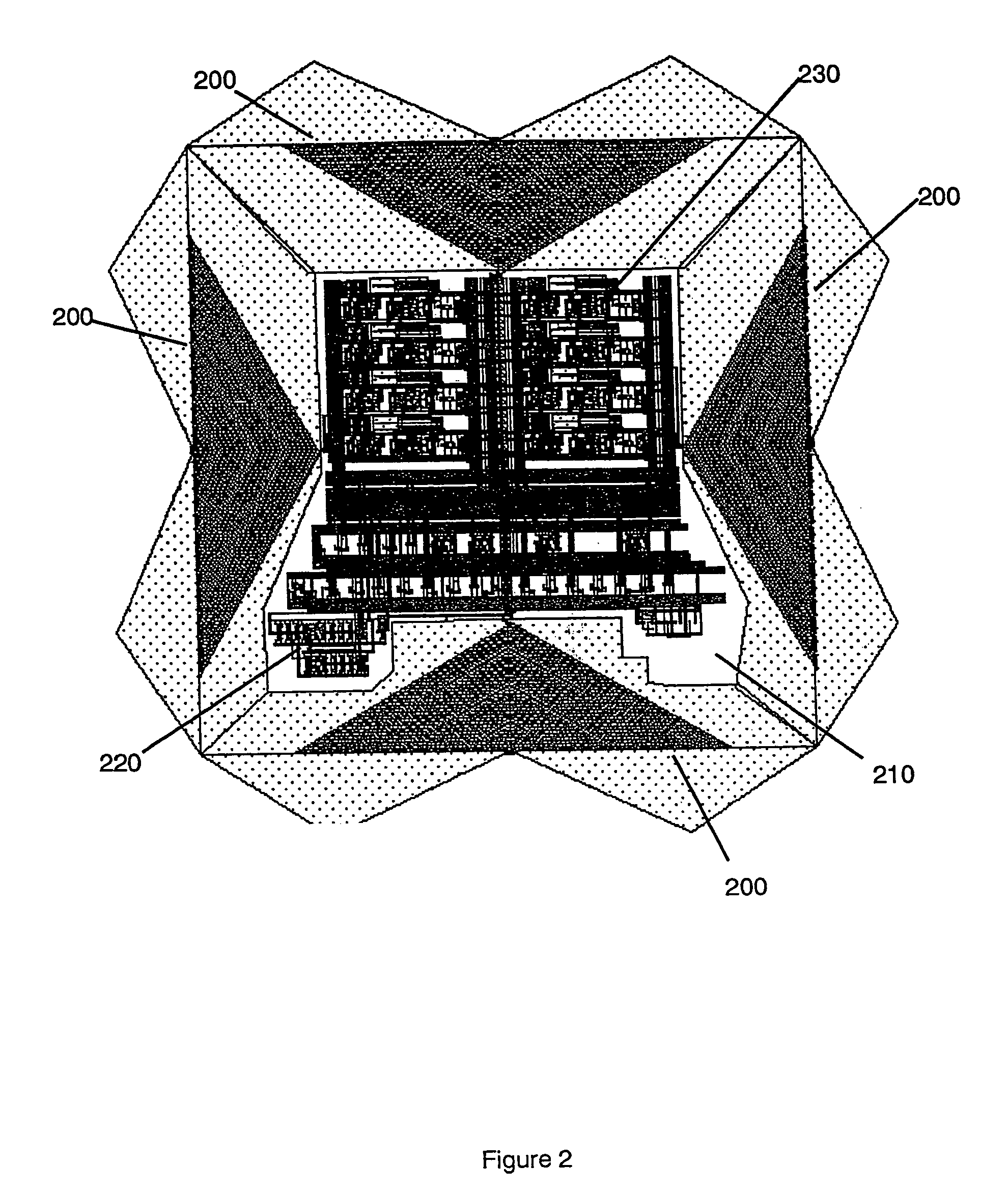
[0105]According to the present invention, a molecular memory integrated circuit apparatus comprises one or more stacked systems each comprising a memory element comprising one or more media surfaces, optional servo tracking marks embedded in the media surface, a positioning mechanism for positioning the media surfaces, a control means for controlling the positioning mechanism, an input / output section which comprises at least one head having a fine tip portion faced towards the memory media surface, a positioning mechanism for positioning the head or heads above the memory media surface or surfaces, a control means for controlling the positioning mechanism, a write section which converts an analog or digital signal to write information, a sense section which converts the input section to analog or digital information, an optional sense section which converts position information to analog or digital information, an optional cleaning section which removes unwanted particles, an option...


PUM

PropertyMeasurementUnit
thicknessaaaaaaaaaa
distanceaaaaaaaaaa
voltageaaaaaaaaaa

Abstract

A molecular memory media having a media surface and a platform with read / write heads. The platform and media are moved to allow one of addition, removal, and repositioning of atoms, electrons, and charges on a surface of the media. The media is a material capable of storing data written to it, and detectable using a vibrating tip sensor that resonates at a free space value which is phase shifted when charges or anomalies on a surface of the media are present. Other methods of reading and writing to the media are presented. The media may be enhanced by augmenting grain boundaries of the media vis deposition and removal of PMMA materials. Servo trenches and sync bits identify positions of the read / write heads and maintain alignment during memory operations.

Description

[0001]This application claims the benefit of prior filed and co-pending United States Provisional application Culver et al., entitled “Molecular Memory Medium and Molecular Memory Integrated Circuit,” and having a series / Ser. No. of 60 / 112,787 filed Dec. 18, 1998.BACKGROUND OF THE INVENTIONField of the Invention[0002]This invention relates to memory reading and writing apparatus. The invention is more particularly related to memory reading and writing apparatus that utilize operations on single atoms or molecules, and groups of atoms or molecules for performing memory reading and writing.REFERENCES[0003]This application incorporates by reference, in their entirety, the following documents:[0004](1) U.S. Pat. No. 5,453,970, (Rust et al.)[0005](2) AFM Fabricates a Tiny Transistor, Science Vol 266, 28 Oct. 1994, p. 543[0006](3) Gold deposition from a scanning tunneling microscope tip, H. J. Mamin, S. Chiang, H. Birk, P. H. Guethner, and D. Rugar, J. Vac. Sci. Tech. B9 (2) March / April 9...

Claims


Application Information

Patent Timeline
Patent Type & Authority Patents(United States)
IPC IPC(8): G11B9/00G01Q80/00G11B5/00G11B5/127G11B5/35G11B5/48G11B9/08G11C13/02
CPCB82Y10/00G11B5/127G11B5/48G11B9/14G11B9/1418G11B9/1454G11B9/1472G11B9/149G11C13/0014G11C13/02G11B5/00Y10S977/947G11B5/35G11B9/08G11B2005/0002G11B2005/0005
Inventor RUST, LEGAL REPRESENTATIVE, THOMAS F.CULVER, DECEASED, JOANNE P.
Owner NANOCHIP
Why Eureka
Try Eureka