Displaying device and electronic apparatus

一种显示装置、电子设备的技术,应用在辨认装置、电路、电气元件等方向,达到高效率充电的效果

Inactive Publication Date: 2004-09-22
BOE TECH GRP CO LTD
View PDF1 Cites 22 Cited by
  • Summary
  • Abstract
  • Description
  • Claims
  • Application Information

AI Technical Summary

Problems solved by technology

This is a common problem not only for liquid crystal display devices, but also for various electronic devices equipped with other display devices.

Method used


Image

  • Displaying device and electronic apparatus
  • Displaying device and electronic apparatus
  • Displaying device and electronic apparatus

Examples


no. 1 Embodiment approach

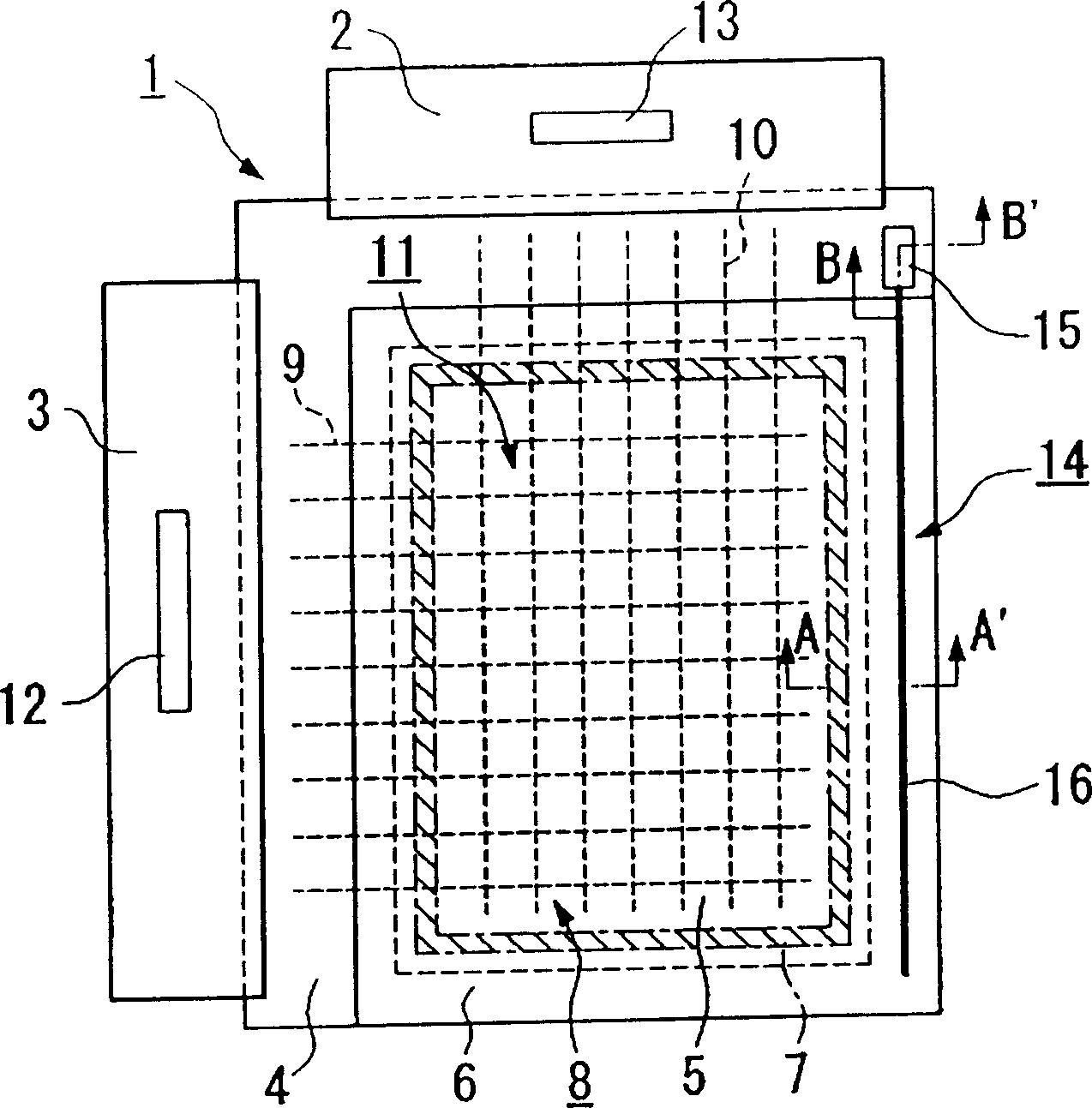
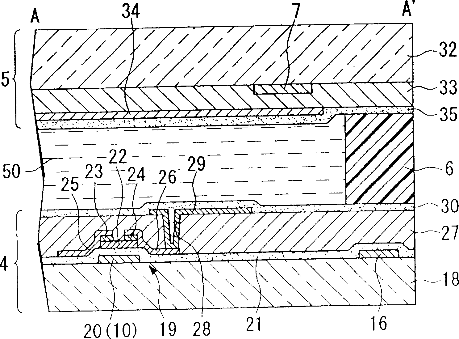
[0109] Below, refer to Figure 1 to Figure 7 The first embodiment of the present invention will be described.

[0110] The display device of the present embodiment is an example of an active matrix transmission (transmission) type liquid crystal display device using amorphous silicon TFTs (thin film transistors) as pixel switching elements.

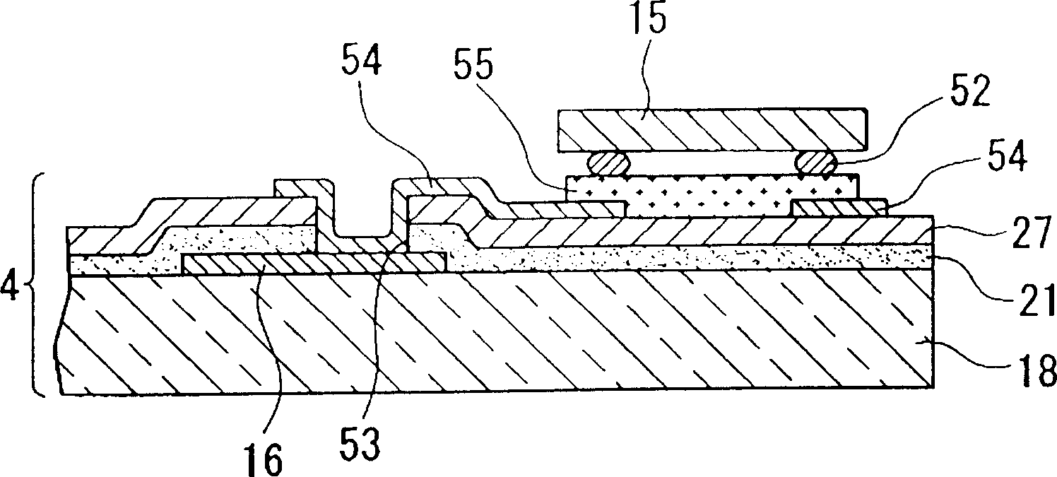
[0111] figure 1 It is a plan view of the liquid crystal display device of this embodiment. figure 2 and image 3 is a diagram showing a cross-sectional structure of a liquid crystal display device, figure 2 is along figure 1 The profile of the line A-A', image 3 is along figure 1 Sectional view of line B-B'. Figure 4 to Figure 6 It is a plan view showing a modified example of the arrangement of the antenna, Figure 7 yes Figure 6 Sectional view of part of the composition. In addition, in each of the following figures, in order to make each constituent element a recognizable size, the ratio of the dimensions is different for...

no. 2 Embodiment approach

[0125] Below, refer to Figure 8 , Figure 9 A second embodiment of the present invention will be described.

[0126] The basic structure of the liquid crystal display device of this embodiment is the same as that of the first embodiment, and only the mounting position of the IC chip and the structure of the accompanying antenna are different.

[0127] Figure 8 It is a plan view of the liquid crystal display device of this embodiment. Figure 9 is a diagram showing a cross-sectional structure of a liquid crystal display device along Figure 8 Sectional view of line C-C'. exist Figure 8 , Figure 9 in, for with Figure 1 to Figure 3 Common constituent elements are assigned the same reference numerals, and detailed descriptions thereof are omitted.

[0128] In the first embodiment, the IC chip 15 is mounted on the element substrate 4 of the liquid crystal cell 1 , and the entirety of the antenna 16 is formed on the element substrate 4 . In contrast, in this embodiment...

no. 3 Embodiment approach

[0134] Below, refer to Figure 10 A third embodiment of the present invention will be described.

[0135] In contrast to the case where the display devices of the first and second embodiments are liquid crystal display devices using amorphous silicon TFTs as pixel switching elements, the display device of this embodiment is a liquid crystal display device using polysilicon or single crystal silicon TFTs as pixel switching elements. device.

[0136] Figure 10 It is a plan view of the liquid crystal display device of this embodiment.

[0137] Amorphous silicon TFTs cannot be used as integrated circuits for communication in IC chips constituting wireless communication devices due to the driving capability of transistors. On the other hand, since polysilicon TFTs and single-crystal silicon TFTs have sufficient drive capability, they can constitute integrated circuits for communication. Therefore, in this embodiment, if Figure 10 As shown, on the element substrate 4, a commu...


PUM


Abstract

To provide a display device and an electronic apparatus including a radio communication device, an embodiment of the radio communication device being an IC tag, which do not need a special space to attach the IC tag and is capable of reducing the amount of time and effort required for attaching the IC tag, a display device including a radio communication device having at least one substrate provided with a display unit and display-unit-driving wiring lines 9 and 10 , a communication integrated-circuit unit, and an antenna is provided. At least a part of the antenna is formed on the substrate and formed of a conductor formed in the same layer as a conductor that constitute the display unit or conductors that constitute the display-unit-driving wiring lines.

Description

technical field [0001] The present invention relates to a display device and electronic equipment provided with a wireless communication device. Background technique [0002] For example, in the field of display devices such as liquid crystal displays, a production method called "manufacturing multiple at the same time" is used: a plurality of patterns for liquid crystal cells are simultaneously produced on one mother substrate, and the Two motherboards are bonded together and then divided into individual cassettes (for example, refer to Patent Document 1). This production method is an excellent method of productivity, but there are many subsequent steps such as connection of a flexible printed circuit board (Flexible Printed Circuit, hereinafter abbreviated as FPC) for driving before the liquid crystal module product is shipped. Especially after being divided into individual boxes, there is a problem that it is difficult to have product identification information such as l...

Claims


Application Information

Patent Timeline
Patent Type & Authority Applications(China)
IPC IPC(8): B42D15/10G02F1/1345G06K19/00G06K19/07G06K19/077G09F9/30G09G3/20G09G3/36G09G5/00
CPCG09G3/3648H01L2924/01019G06K19/07749G09G3/20G09G2380/04H01L2924/3025H01L2224/16H01L2924/00014H01L2224/0401B28B1/0873B28B3/021B28B7/0055B28B7/007B28B7/0097B28B7/162B28B7/241E02D29/02
Inventor 佐藤尚
Owner BOE TECH GRP CO LTD
Why Eureka
Try Eureka