Semiconductor device and producing method, semiconductor package, electronic device and producing method, electronic instrment

A technology of electronic equipment and semiconductors, which is applied in the direction of semiconductor devices, semiconductor/solid-state device manufacturing, semiconductor/solid-state device components, etc.

Inactive Publication Date: 2004-09-29
SEIKO EPSON CORP
View PDF1 Cites 21 Cited by
  • Summary
  • Abstract
  • Description
  • Claims
  • Application Information

AI Technical Summary

Problems solved by technology

Contents of the invention

Method used


Image

  • Semiconductor device and producing method, semiconductor package, electronic device and producing method, electronic instrment
  • Semiconductor device and producing method, semiconductor package, electronic device and producing method, electronic instrment
  • Semiconductor device and producing method, semiconductor package, electronic device and producing method, electronic instrment

Examples


Embodiment Construction

[0061] Hereinafter, semiconductor devices, electronic devices and their manufacturing methods according to embodiments of the present invention will be described with reference to the drawings.

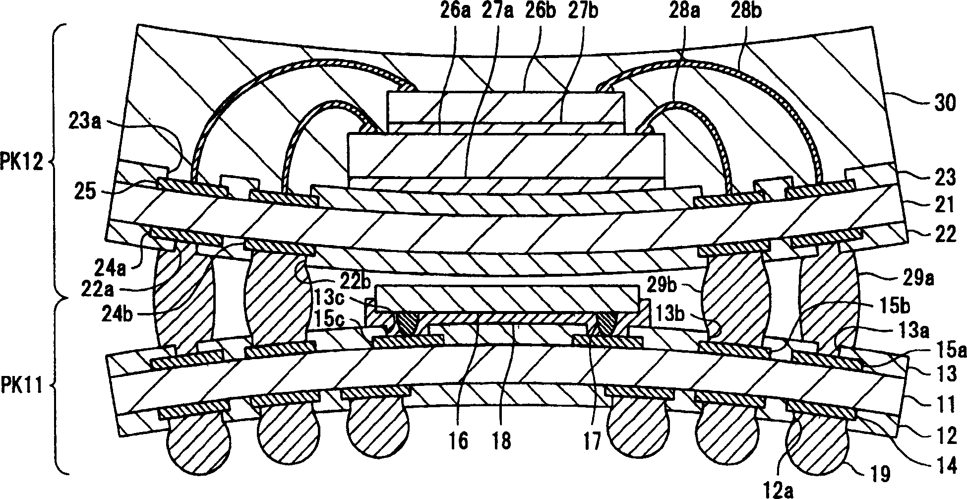
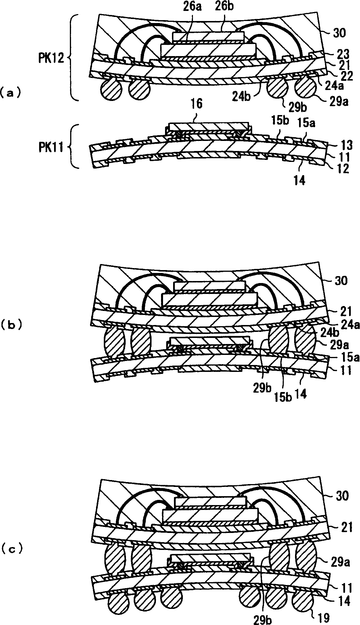
[0062] figure 1 It is a cross-sectional view showing the structure of the semiconductor device according to the first embodiment of the present invention.

[0063] In the first embodiment, the opening diameters of both the openings 13a, 13b and the openings 22a, 22b of the semiconductor packages PK11, PK12 to which the protruding electrodes 29a, 29b are bonded are changed.

[0064] exist figure 1 Among them, a carrier substrate 11 is provided on the semiconductor package PK11. Furthermore, a land surface 14 for disposing the protruding electrodes 19 is provided on the inner surface of the carrier substrate 11 . In addition, an insulating film 12 such as a solder resist is formed on the back surface of the carrier substrate 11 on which the land 14 is provided, and an opening 12 a ex...


PUM


Abstract

A method is provided to enhance the connection reliability in three-dimensional mounting while considering the warping of packages. Opening diameters of the openings provided corresponding to protruding electrodes, respectively, are set so as to gradually decrease from the central portion toward the outer peripheral portion of a carrier substrate, and the opening diameters of openings provided corresponding to the protruding electrodes, respectively, are set so as to gradually decrease from the central portion toward the outer peripheral portion of another carrier substrate.

Description

technical field [0001] The present invention relates to a semiconductor device, a semiconductor package, an electronic device, an electronic device, a method for manufacturing a semiconductor device, and a method for manufacturing an electronic device, and is particularly applicable to a stacked structure of a semiconductor package or the like. Background technique [0002] In conventional semiconductor devices, in order to achieve three-dimensional mounting of semiconductor chips, there is a method of stacking semiconductor chips with metal balls interposed therebetween, as disclosed in Patent Document 1, for example. [0003] 【Patent Document 1】 [0004] Japanese Patent Laid-Open Publication No. 11-307717 [0005] However, when the semiconductor chip is mounted on the package, warpage occurs in the package due to the difference in linear expansion coefficient or the like between the semiconductor chip and the package. For this reason, in the method of stacking packages w...

Claims


Application Information

Patent Timeline
Patent Type & Authority Applications(China)
IPC IPC(8): H01L25/18H01L21/60H01L23/498H01L25/10H01L25/11H05K1/18
CPCH01L2225/1058H01L2224/45124H05K1/181H05K2201/1053H01L2924/3511H05K2201/10515H01L2224/16H01L2924/15311H01L2225/1023H01L2924/01029H01L2224/48091H01L2924/01013H01L2224/32225H01L2224/48225H01L2924/15331H01L2225/06568H01L2224/73204H01L24/48H01L2924/01079H01L2224/48465H05K2201/10734H01L2224/48227H01L25/105H01L2224/32145H01L23/49816H01L2224/45144H01L25/0657H01L2224/16225H01L2224/73265H01L24/45H01L24/73H01L2924/00014H01L2924/181Y02P70/50H01L2924/00012H01L2924/00H01L2224/05599
Inventor 青栁哲理
Owner SEIKO EPSON CORP
Why Eureka
Try Eureka