Open wafer box before prevetion of outgassing pollution and method for preventing outgassing pollution

A front-opening wafer box, wafer box technology, applied in the direction of electrical components, semiconductor/solid-state device manufacturing, circuits, etc., can solve the problem of reducing the yield of products, and achieve the effect of simple application, simple structure and cost saving

Inactive Publication Date: 2004-10-13
POWERCHIP SEMICON CORP
View PDF0 Cites 9 Cited by
  • Summary
  • Abstract
  • Description
  • Claims
  • Application Information

AI Technical Summary

Problems solved by technology

Therefore, when the wafer is processed and put back into the front-opening wafer cassette, if the processed wafer produces outgassing, the gas (such as phosphorus gas) diffused from the wafer will fill the front opening. The inside of the open wafer box will contaminate other unprocessed wafers in the wafer box, resulting in a decrease in the good rate of the product

Method used


Image

  • Open wafer box before prevetion of outgassing pollution and method for preventing outgassing pollution
  • Open wafer box before prevetion of outgassing pollution and method for preventing outgassing pollution
  • Open wafer box before prevetion of outgassing pollution and method for preventing outgassing pollution

Examples


Embodiment Construction

[0018] In order to make the above and other purposes, features, and advantages of the present invention more comprehensible, a preferred embodiment is specifically cited below, together with the accompanying drawings, as follows:

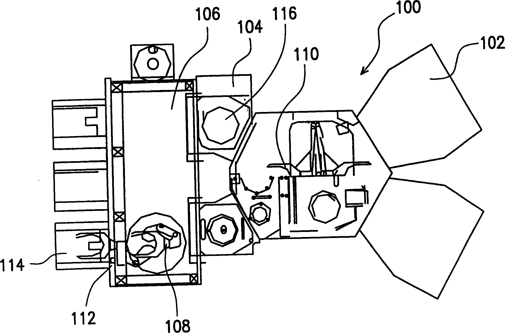
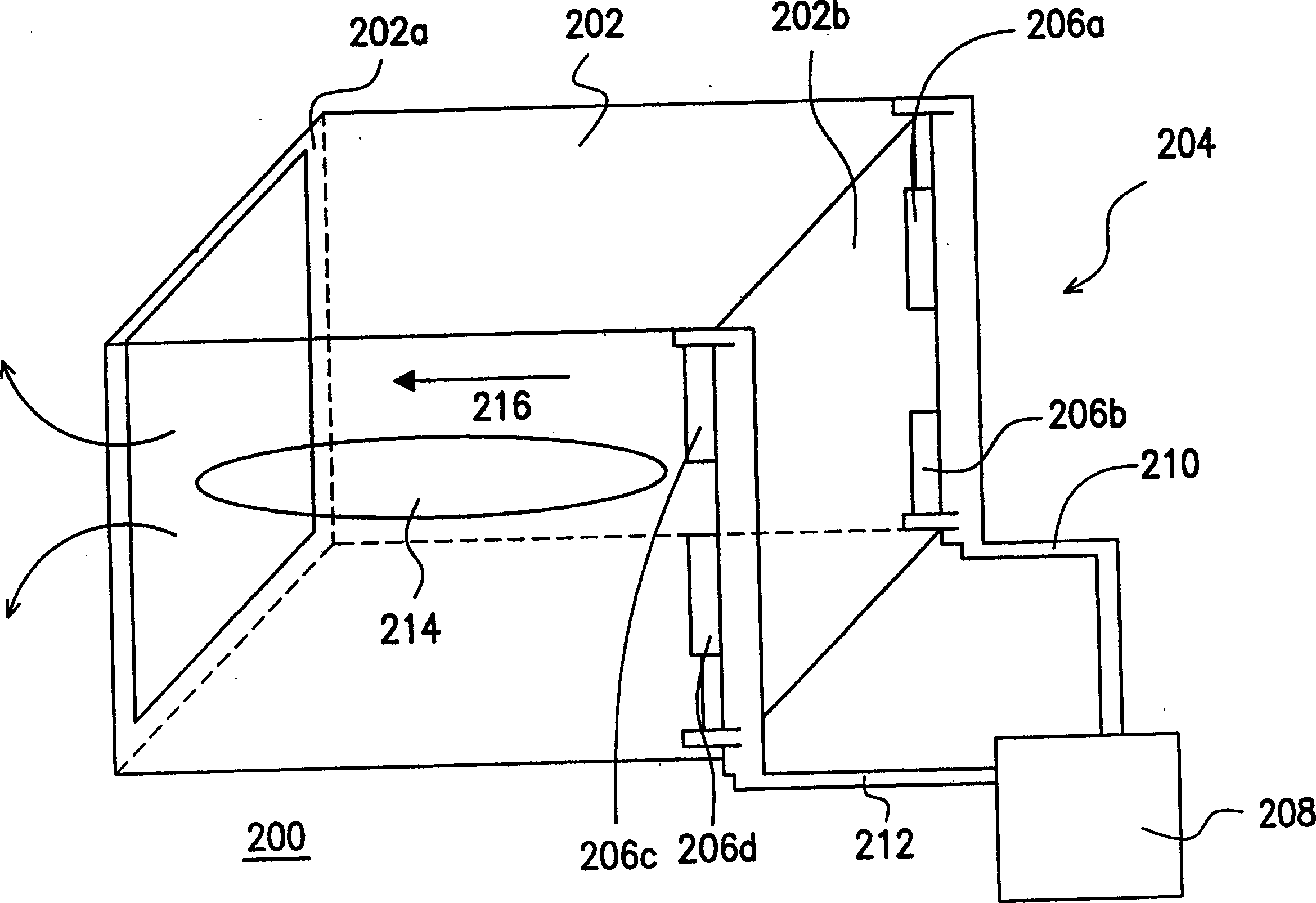
[0019] figure 2 It is a schematic diagram showing the three-dimensional structure of the front opening wafer cassette of the present invention.

[0020] Please refer to figure 2 As shown, the FOUP 200 of the present invention includes a FOUP body 202 and a cleaning device 204 . The cleaning device 204 is constituted by, for example, blowing members 206 a to 206 d , a gas supply device 208 , and pipes 210 and 212 .

[0021] The air blowing members 206a-206d are arranged inside the FOUP body 202, and a plurality of air blowing members 206a-206d are arranged at the opening of the FOUP body 202 in a staggered manner, for example, at intervals. 202a is opposite to the left and right sides of the bottom plate 202b. For example, the blowing component...


PUM


Abstract

A kind of former-opening wafer box that is able to avoid venting gas is at least composed of the former-opening wafer box body and cleanliness setting. The former-opening wafer box itself has hatch part and bottom board, the bottom board and the hatch part face to face. Cleanliness setting at least have huff component set up in the former-opening wafer box and gas providing installation that link huff component and supply gas to the huff component.

Description

technical field [0001] The present invention relates to a semiconductor manufacturing process and equipment, and in particular to a method for avoiding outgas pollution before opening a wafer box and avoiding outgas pollution. Background technique [0002] With the increasing integration of semiconductor elements in integrated circuits, the relative accuracy of the manufacturing process is extremely important. Because once a slight error (Error) or contamination occurs in the manufacturing process, it may cause the failure of the manufacturing process, resulting in damage or scrap of the wafer, thus consuming a lot of cost. [0003] In the general semiconductor manufacturing process, the semiconductor manufacturing machine is composed of several modules (process / transmission / storage / safety chain / reaction gas), and the wafer is processed by the wafer transfer system (Wafer Transfer System). Transfer between modules and storage modules. The transfer of the wafer is to use th...

Claims


Application Information

Patent Timeline
Patent Type & Authority Applications(China)
IPC IPC(8): H01L21/00H01L21/68
Inventor 吴荣原黄国华
Owner POWERCHIP SEMICON CORP
Why Eureka
Try Eureka