

Grid structure from material with high dielectric constant and preparing technique
A technology of high dielectric constant material and preparation process, applied in circuits, electrical components, semiconductor/solid-state device manufacturing, etc., can solve the problems of loss of switching characteristics and large gate leakage current of CMOS transistors, and achieve good interface characteristics and reliability. sexual effect
- Summary
- Abstract
- Description
- Claims
- Application Information
AI Technical Summary
Problems solved by technology
Method used
Image

Examples
Embodiment 1
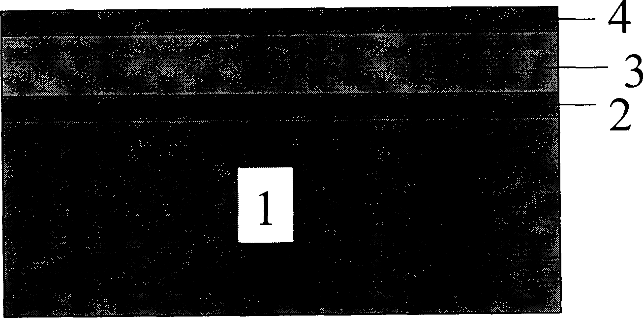
[0014] 1. Use the rapid annealing furnace RTO (or conventional oxidation furnace), the furnace temperature is 900 ° C, in NO (or N 2 O) in the gas, on the surface of a clean silicon wafer, oxidize and grow a silicon oxynitride (SiON) film of about 10 Å;
[0015] 2. Deposit 30 Å of high dielectric constant (high-k) material, such as HfO, on the SiON layer by CVD (MOCVD, ALCVD, etc.) 2 or HfSi x o y or HfAl x o y Wait.
[0016] 3. Deposit a layer of ultra-thin silicon nitride (SiN) on the high dielectric constant material layer by CVD (MOCVD, ALCVD, etc.), with a thickness of about 10 Å.
Embodiment 2
[0018] 1. Use the rapid annealing furnace RTO, the furnace temperature is about 1000°C, and grow a 5 Å SiON film on the surface of the clean silicon wafer in NO gas;
[0019] 2. Deposit 5 Å of high dielectric constant material, such as Al, on the SiON layer by CVD (MOCVD or ALCVD) method 2 o 3 or ZrO 2 or Ta 2 o 5 Wait.
[0020] 3. Using CVD (MOCVD or ALCVD) to deposit an ultra-thin SiN layer on the high dielectric constant material layer with a thickness of 15 Å.
Embodiment 3
[0022] 1. Use a conventional oxidation furnace, the furnace temperature is about 800 ° C, in N 2 In O gas, oxidize and grow a 15 Å SiON film on the surface of a clean silicon wafer;
[0023] 2. Deposit 60 Å of high dielectric constant material, such as HfO, on the SiON layer by CVD method 2 or Al 2 o 3 Wait.
[0024] 3. Treat the surface of the prepared high dielectric constant material layer with nitrogen plasma to form a thin layer of silicon nitride (SiN) on the surface with a thickness of 3 Å.
[0025] The sandwich gate structure prepared in the above examples, the SiON layer can effectively isolate the diffusion between the impurity elements in the high dielectric constant material and the silicon substrate, and has very good interface characteristics and reliability; the SiN layer can Play the role of high dielectric constant material and polysilicon interface layer, and can block from P + Polycrystalline boron penetration.
PUM
 Abstract
Description
Claims
Application Information