Grid structure of high-K material based on silicon-on-insulator (SOI) substrate and preparation method thereof

A high dielectric constant material and high dielectric constant technology, applied in the direction of circuits, electrical components, semiconductor devices, etc., can solve the problems of not having, reducing the electron mobility of devices, etc.

Inactive Publication Date: 2011-01-19
SHANGHAI INST OF MICROSYSTEM & INFORMATION TECH CHINESE ACAD OF SCI
View PDF7 Cites 0 Cited by
  • Summary
  • Abstract
  • Description
  • Claims
  • Application Information

AI Technical Summary

Problems solved by technology

[0004] However, the substrate it uses is Si, which does not have the above-mentioned advantages of using the SOI substrate. In addition, the patent grows SiON directly on the substrate, and a layer of SiN grown on the high dielectric constant material l

Method used


Image

  • Grid structure of high-K material based on silicon-on-insulator (SOI) substrate and preparation method thereof
  • Grid structure of high-K material based on silicon-on-insulator (SOI) substrate and preparation method thereof

Examples


Embodiment 1

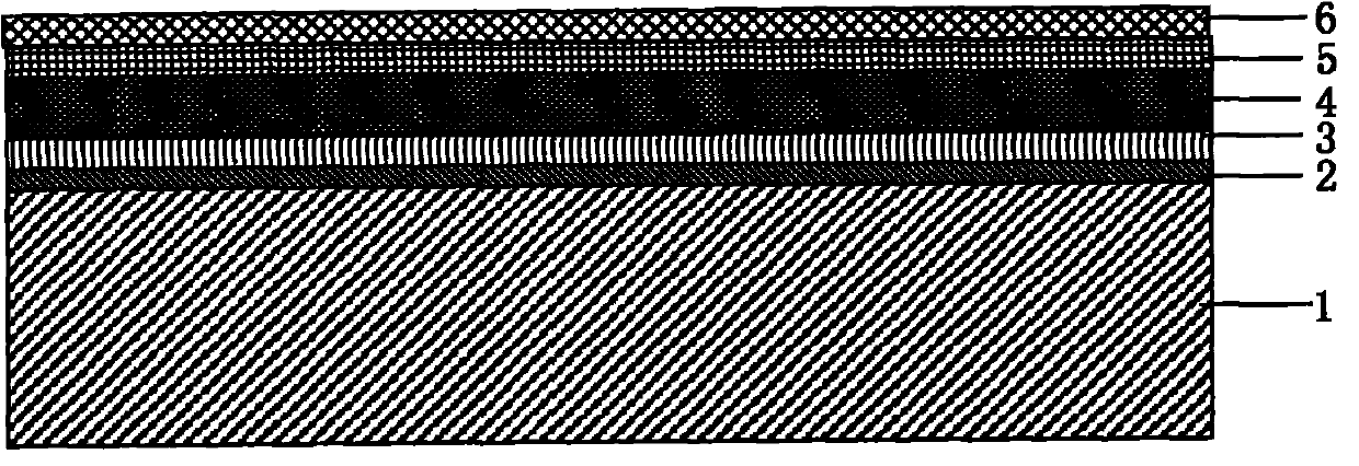
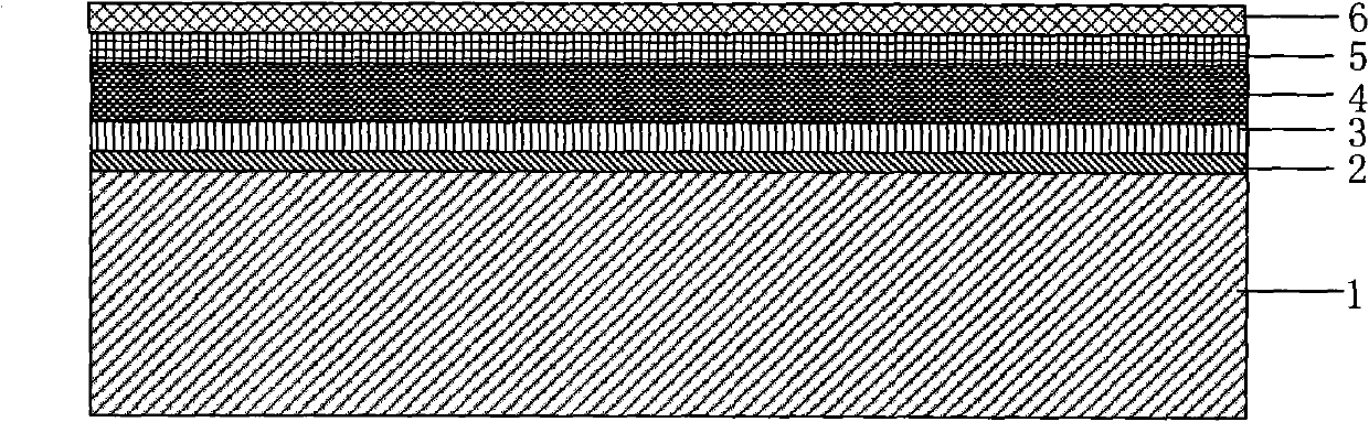
[0018] Please refer to shown in Fig. 1, a kind of high dielectric constant material gate structure based on SOI substrate comprises the SiO that is positioned on SOI substrate 1 2 Layer 2, on SiO 2 Si on layer 3 N 4 Layer 3, located in Si 3 N 4 The high dielectric constant oxide layer 4 on the high dielectric constant oxide layer, the high dielectric constant oxynitride layer 5 on the high dielectric constant oxide layer, and the metal gate electrode 6 on the high dielectric constant oxynitride layer.

[0019] A method for preparing a high dielectric constant material gate structure based on an SOI substrate, the method comprising the following steps:

[0020] Step 1, cleaning and drying, put the cut SOI substrate into the first solution and ultrasonically clean it for 15 minutes to remove metal contaminants on the substrate surface, then rinse with deionized water, and then put the substrate into the diluted second solution In solution (volume ratio: HF:H 2 O=1:50) for ...

Embodiment 2

[0034] In this embodiment, cleaning or drying may not be performed (step 1 is omitted), and the cut SOI substrate is directly processed in step 2 by PEALD process, and then processed by steps 3-5 by ALD process. Other processing steps in this embodiment are the same as in Embodiment 1.


PUM

PropertyMeasurementUnit
Thicknessaaaaaaaaaa

Abstract

The invention discloses a method for preparing multiple layers of grid structures of high-K material on silicon-on-insulator (SOI) material. The method comprises the following steps: pretreating the surface of the SOI through O2 plasmas, and then forming an ultrathin SiO2 interface layer on the surface of a SOI substrate; subsequently, growing a layer of ultrathin Si3N4 on the ultrathin SiO2 interface layer by utilizing an atom layer decomposition (ALD) mode, and the layer of ultrathin Si3N4 can effectively isolate diffusion between impurity elements in the high-K material layer and silicon on the top layer of SOI and prevent regrowth of the SiO2 layer at the lower part during later thermal treatment; subsequently, depositing a layer of high-K material on Si3N4, carrying out proper nitrogen treatment on the high-K material so as to form a layer of oxyntride having high-K, and the layer of oxyntride can effectively prevent diffusion of elements between a metal grid electrode and the high-K material layer; and finally, growing a metal electrode in a sputtering mode.

Description

technical field [0001] The invention relates to a gate structure of high dielectric constant material based on an SOI substrate and a preparation method thereof, belonging to the technical field of microelectronics and solid electronics. Background technique [0002] With the rapid development of microelectronics technology, the research and development of high-performance, high-integration, and multi-functional ICs have increasingly stringent requirements on materials. Silicon-on-insulator SOI (Silicon-on-insulator SOI) materials are new silicon-based integrated circuit materials. , known as "the new silicon-based integrated circuit technology in the 21st century", compared with bulk silicon, SOI has the advantages of no latch, high speed, low voltage, low power consumption and radiation resistance. In addition, with the continuous reduction of device feature size, in order to ensure that the gate has a good control ability over the channel, SiO 2 The thickness of the gate...

Claims


Application Information

Patent Timeline
IPC IPC(8): H01L29/51H01L21/28
Inventor 程新红徐大伟王中健何大伟宋朝瑞俞跃辉
Owner SHANGHAI INST OF MICROSYSTEM & INFORMATION TECH CHINESE ACAD OF SCI
Why Eureka
Try Eureka