Integrated circuit structure for mixed-signal RF applications and circuits

A technology of integrated circuits and electrical signals, which is applied to circuits, electrical components, and electrical solid-state devices. The effect of parasitic capacitance

Inactive Publication Date: 2004-11-17
FREESCALE SEMICON INC
View PDF1 Cites 7 Cited by
  • Summary
  • Abstract
  • Description
  • Claims
  • Application Information

AI Technical Summary

Problems solved by technology

This coupling reduces the quality factor
In addition, eddy curren

Method used


Image

  • Integrated circuit structure for mixed-signal RF applications and circuits
  • Integrated circuit structure for mixed-signal RF applications and circuits
  • Integrated circuit structure for mixed-signal RF applications and circuits

Examples


Embodiment Construction

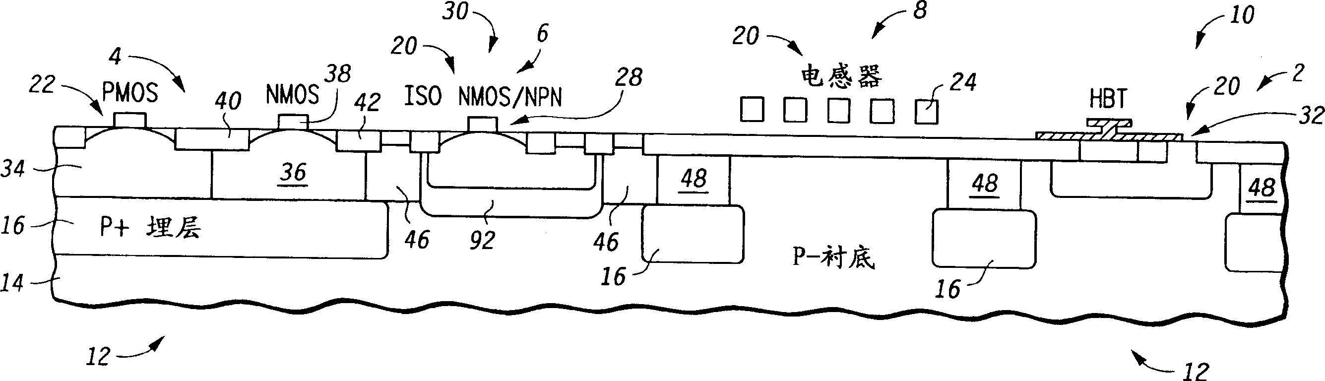
[0020] With reference to the drawings by reference character, figure 1 A cross-section of an integrated circuit (IC) 2 fabricated in accordance with a preferred embodiment of the present invention in a p-type substrate is depicted. For n-type substrates, the n-type buried layer will replace the p-type buried layer. Such as figure 1 As shown, IC2 supports digital part 4, analog part 6, passive RF part 8 and active RF part 10. IC 2 is capable of supporting digital 4 , analog 6 , passive 8 , and active 10 RF components having an isolation structure 12 that reduces electrical interaction between different components via a high-resistivity substrate 14 . In the circuit, substrate 14 is essentially a resistor connecting all devices on IC2. By isolating and isolating these various components, it is possible to integrate digital components 4, analog components 6, passive RF components 8 and active RF components 10 on a single IC2. Strategic placement of these components in or on t...


PUM


Abstract

An integrated circuit (12) that supports digital circuits (4), analog circuits(6), and RF circuits (8) on a single IC. Digital CMOS circuitry lies on a low resistivity layer (16) that provides good latch-up qualities and allows for dense PAD I/O. Analog CMOS circuitry rests on an isolated well region (20) on a highly resistive layer (14) in order to minimize signal crosstalk through the substrate. Analog BJT devices also sit on a highly resistive region (14) within its own well structure (20) in order to minimize parasitic capacitances and provide for high frequency device switching. RF passive elements, such as inductors and capacitors, rest on a highly resistive region (14) in order to minimize signal losses that especially occur at high frequencies. RF active components rest on a highly resistive region to maximize device performance.

Description

technical field [0001] This invention relates to the field of integrated circuits, and more particularly, to integrated circuits supporting digital, analog and radio frequency (RF) circuits on a single microchip. Background technique [0002] There is a strong need for monolithic integrated circuits (ICs) that can support digital, analog, and radio frequency (RF) circuit elements. By integrating each of these circuit types onto a single IC, it is possible to greatly improve the quality and cost of portable RF devices for wireless and optical communication applications. However, the integration of these different circuit types presents several unique issues. [0003] For example, disposing each of these different device types on a monolithic IC often results in inter-circuitry interaction via the IC substrate. This interaction can greatly degrade and inhibit the desired operation of the IC when digital, analog and RF circuit elements are provided on the same substrate. [...

Claims


Application Information

Patent Timeline
IPC IPC(8): H01L21/822H01L21/8249H01L23/522H01L27/04H01L27/06H01L27/08
CPCH01L27/0617H01L27/08H01L2924/3011H01L23/5227H01L27/0635H01L21/8249H01L2924/0002H01L2924/00H01L27/10
Inventor 黄文伶詹姆斯·基希格斯纳戴维·J·蒙克
Owner FREESCALE SEMICON INC
Why Eureka
Try Eureka