Preparation method of white organic electroluminescent device

An electroluminescence and electromechanical technology, applied in the field of preparation of white organic electroluminescence devices, can solve the problems of lack of spectral stability and poor spectral stability.

Inactive Publication Date: 2005-01-26
中科应化(长春)科技有限公司
View PDF0 Cites 15 Cited by
  • Summary
  • Abstract
  • Description
  • Claims
  • Application Information

AI Technical Summary

Problems solved by technology

In 2002, Y.Wang et al. further improved the efficiency of white light organic light-emitting devices made of fluorescent organic molecules. Using a simple-structured double-layer device, the maximum electroluminescent efficiency reached 6.5cd / A (3.6Lm / W), The device achieves white light emission through excimer complexes formed between organic layers, but such white light devices usually do not have good spectral stability
But there is also the problem of poor spectral stability

Method used


Image

  • Preparation method of white organic electroluminescent device
  • Preparation method of white organic electroluminescent device
  • Preparation method of white organic electroluminescent device

Examples


Embodiment 1

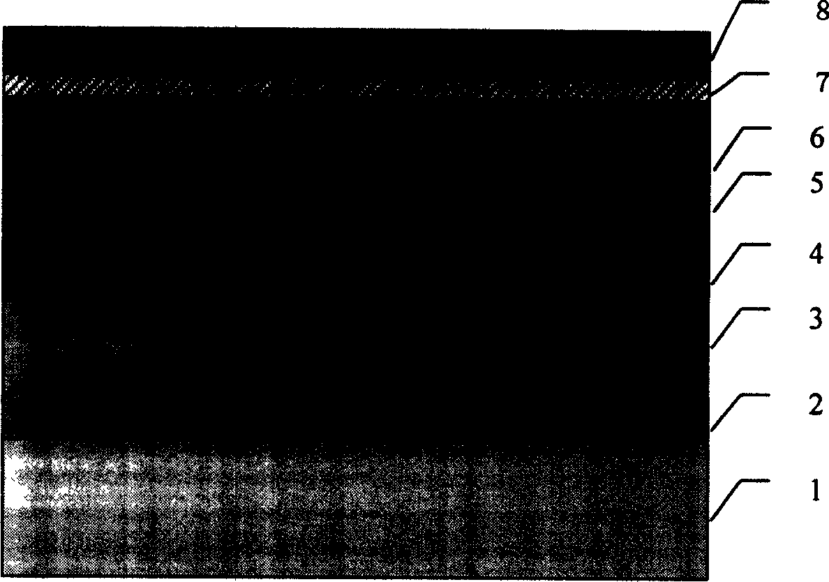
[0043] Doping DCJTB into NPB as a light-emitting layer to prepare a structure of ITO / NPB / DCJTB: NPB / NPB / BCP / Alq 3 / LiF / Al electroluminescent device, in a vacuum of 10 -4 Evaporate the organic and metal electrode layers under the pressure of Pa, the evaporation rate of the organic layer is controlled at 2 Å / s, the evaporation rate of LiF is controlled at 0.5 Å / s, the evaporation rate of the metal is controlled at 5 Å / s, and the doping concentration Controlled at 1%, among them, NPB layer thickness is 30~35nm, DCJTB: NPB layer is 3~5nm, NPB layer is 8~10nm, BCP layer is 9~10nm, Alq 3 The thickness of the LiF layer is 25-30nm, the thickness of the LiF layer is 0.8-1.5nm, and the thickness of the Al layer is 80-100nm. The obtained device is driven by DC voltage, and white light can be obtained. The maximum current efficiency is 3.15cd / A, and the maximum brightness is 3669cd / m 2 .

Embodiment 2

[0045] Doping DCJTB and TPB into NPB as the light-emitting layer is prepared into a structure of ITO / NPB / DCJTB: NPB / TPB: NPB / BCP / Alq 3 / LiF / Al electroluminescent device, in a vacuum of 10 -4 The organic and metal electrode layers were evaporated under the pressure of Pa, the evaporation rate of the organic layer was controlled at 2 Å / s, the evaporation rate of LiF was controlled at 0.5 Å / s, and the evaporation rate of metal was controlled at 5 Å / s. The concentration is controlled at 1%, among which, the thickness of NPB layer is 25-30nm, DCJTB: NPB layer is 8-10nm, TPB: NPB layer is 9-10nm, BCP layer is 8-10nm, Alq 3 The thickness of the LiF layer is 25-30nm, the thickness of the LiF layer is 0.8-1.5nm, and the thickness of the Al layer is 80-100nm. The obtained device is driven by DC voltage, and white light can be obtained. The maximum current efficiency is 4.33cd / A, and the maximum brightness is 6183cd / m 2 .

Embodiment 3

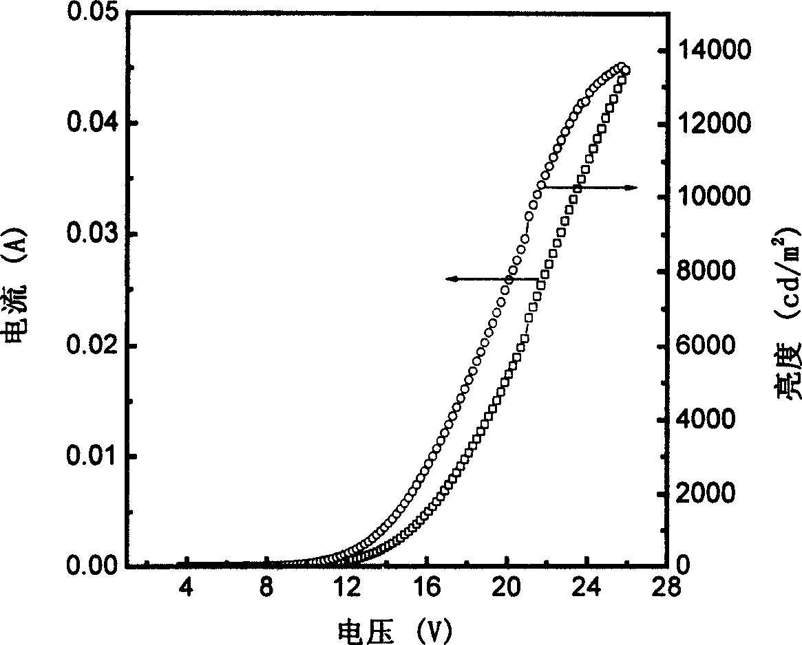
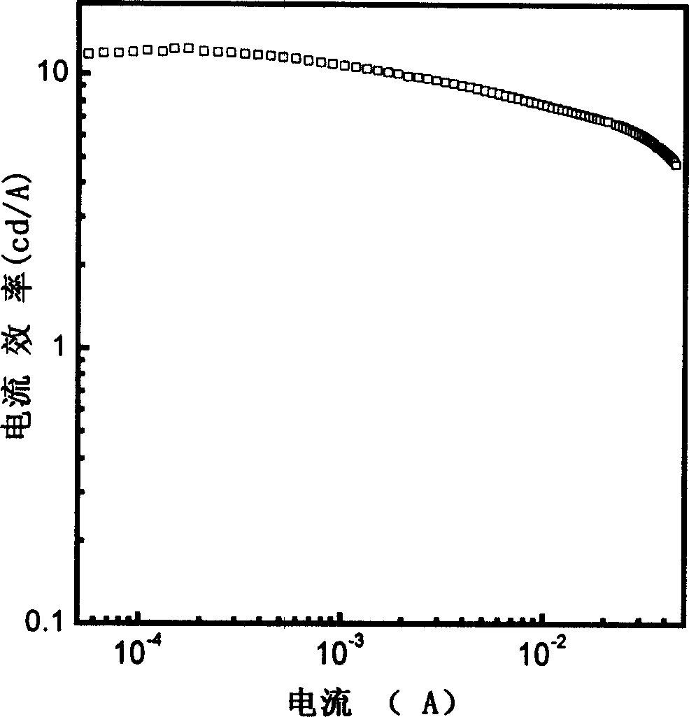
[0047] Doping DCJTB into NPB as a light-emitting layer to prepare a structure of ITO / NPB / DCJTB: NPB / NPB / DNA / BCP / Alq 3 / LiF / Al electroluminescent device, in a vacuum of 10 -4 Evaporate the organic and metal electrode layers under the pressure of Pa, the evaporation rate of the organic layer is controlled at 2 Å / s, the evaporation rate of LiF is controlled at 0.5 Å / s, the evaporation rate of the metal is controlled at 5 Å / s, and the doping concentration Controlled at 1%, among them, NPB layer thickness is 25-30nm, DCJTB: NPB layer is 8-10nm, NPB layer is 4-6nm, DNA layer is 4-5nm, BCP layer is 9-10nm, Alq 3 The thickness of the LiF layer is 25-30nm, the thickness of the LiF layer is 0.8-1.5nm, and the thickness of the Al layer is 80-100nm. The obtained device is driven by DC voltage, and white light can be obtained. The maximum efficiency is 10.3cd / A, and the maximum brightness is 10800cd / m 2 .


PUM


Abstract

The invention discloses a producing method of organic white light device, mixing red light dye and / or green dye or blue dye into cavity transporting material by 1% chroma at the same time, to mixing into cavity transporting material and electric transporting material, producing structure of indium stannum oxide / NPB / DCJTB:C545T:NPB(or DCJTB: NPB) / NPB( or TPB:NPB) / DNA / BCP / Alq3(or C545T:Alq3) / LiF / mental electrode EL device, the device is drived by direct current, and getting white light with color coordinate 0.329, 0.332, the biggest electroluminescence efficiency is 12.4 cd / A, the biggest luminescence brightness is 13550cd / sq m.

Description

technical field [0001] The invention relates to a preparation method of a white organic electroluminescence device. Background technique [0002] In recent years, organic electroluminescent display has been widely studied as the hottest emerging display technology in the flat panel display industry. For organic light-emitting display applications, color display is the ultimate goal that people pursue. Using simple white light and color filters to form red, green and blue three-primary color pixels is an important method for realizing organic color display. In addition to being used for color displays, this ultra-thin white organic light-emitting device is also an ideal light source for liquid crystal backgrounds and future lighting. However, the efficiency and brightness of organic light-emitting display devices and their spectral stability are far from meeting the requirements of applications. Therefore, how to solve the above problems from the design of materials and dev...

Claims


Application Information

Patent Timeline
Patent Type & Authority Applications(China)
IPC IPC(8): H05B33/10H05B33/12
Inventor 马东阁郭法文周全国
Owner 中科应化(长春)科技有限公司
Why Eureka
Try Eureka