
Semiconductor device

A semiconductor and device technology, applied in the field of semiconductor devices equipped with protection devices to prevent electrostatic discharge damage, can solve the problems of different leakage currents of transistors, brightness changes, etc.

Inactive Publication Date: 2010-06-23
SEMICON ENERGY LAB CO LTD
View PDF6 Cites 0 Cited by
  • Summary
  • Abstract
  • Description
  • Claims
  • Application Information

AI Technical Summary

Problems solved by technology

Therefore, even when the same signal voltage is input, the leakage current of transistors in each pixel is different, resulting in variations in luminance

Method used


Image

  • Semiconductor device
  • Semiconductor device
  • Semiconductor device

Examples


Embodiment approach 1

[0091] Refer to the following Figure 3-5 , 10, 11, 18, 19 to describe Figures 1A-1I and embodiments of mask layouts for pixels shown in 2A and 2B.

[0092] refer to image 3 said to be equivalent to Figure 2A A layout of pixels of an equivalent circuit diagram in which a resistor element is used as a protection device is shown. image 3 The pixel shown includes a signal line 8001, a power supply line 8002, scanning lines 8003 and 8004, a switching transistor 8005, an erasing transistor 8006, a drive transistor 8007, a current control transistor 8008, a pixel electrode 8009, a light emitting area 8010, and a power supply line 8011 , a capacitor 8012, and a resistor element (resistor) 8013. The signal line 8001 and the power lines 8002 and 8011 are composed of the same layer of conductive material. Also, scan lines 8003 and 8004 are composed of the same layer of conductive material.

[0093] Figure 18 show image 3 Another example of the mask layout of , in which auxi...

Embodiment approach 2

[0101] In this embodiment, refer to Figure 6A and 6B to describe Figure 3-5 The cross-sectional structure of the driving transistor and light-emitting element shown.

[0102] Figure 6A is a sectional view showing a drive transistor 9021 which is a P-type transistor and a light emitting element 9022 from which light is emitted in the direction of an anode 9023 . The anode 9023 of the light emitting element 9022 is electrically connected to the driving transistor 9021, and an electroluminescent layer 9024 and a cathode 9025 are laminated on the anode 9023 in this order. The cathode 9025 may be composed of a well-known material as long as the material is a light-reflective conductive film with a low work function. For example, Ca, Al, CaF, MgAg, AlLi, etc. are preferably used as the cathode 9025. The electroluminescent layer 9024 may consist of a single layer or multiple layers. In the case of forming a multilayer electroluminescent layer 9024, a hole injection layer, a ...

Embodiment approach 3

[0109] In the case where the semiconductor device of the present invention is operated by a digital driving method, it is preferable to use time gray scale to display an image with multi-level gray scale. In this embodiment, time grayscale is described. Figure 7A is a time graph, the ordinate represents the scan line, and the abscissa represents time. Figure 7B is the timing diagram of the j-th scan line.

[0110]The semiconductor device here has a frame frequency of about 60 Hz. That is, writing of image data is performed 60 times per second, and a period in which an image is written once is called a frame period. In time grayscale, one frame period is divided into subframe periods. The number of divisions is in many cases equal to the number of bits, which is described here for simplicity. That is, as in the present embodiment, 5-bit gradation is shown as an example, and one frame period is divided into 5 subframe periods SF1-SF5. Each subframe period includes an addr...


PUM


Abstract

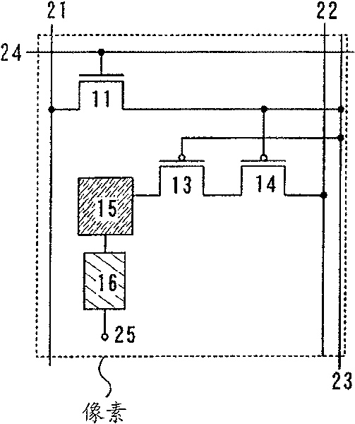
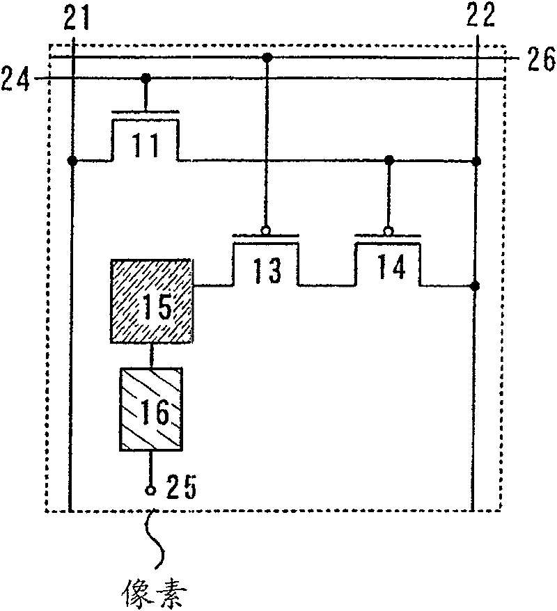
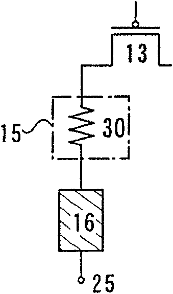
A semiconductor device in which electrostatic discharge damage during manufacturing steps is prevented. More specifically, a semiconductor device in which electrostatic discharge damage during a step in which the formation of a pixel electrode is completed is prevented. A semiconductor device of the invention comprises a light emitting element, a driving transistor and a protection means disposedbetween the light emitting element and the driving transistor. The protection means comprises as least one of a resistor element, a capacitor element and a rectifier element. More specifically, the protection means is disposed between a pixel electrode of the light emitting element and a source electrode or a drain electrode of the driving transistor. It is to be noted that the rectifier element is an element having a rectifying function and corresponds to a diode or a transistor whose drain electrode and gate electrode are connected to each other.

Description

technical field [0001] The present invention relates to a semiconductor device using a semiconductor element such as a transistor, and more particularly to a semiconductor device equipped with a protection device against electrostatic discharge damage. Background technique [0002] Static electricity is formed due to friction, contact, etc. with air and objects such as conductors, semiconductors, and insulators. Electrostatic discharge is caused when excess charge is present on these materials, and when this occurs on free nodes such as input terminals, delicate semiconductor elements formed on the substrate are degraded or damaged. This is known as electrostatic discharge damage. In order to prevent such electrostatic discharge damage, a circuit formed on a substrate (hereinafter referred to as an internal circuit) is connected to an external IC (hereinafter referred to as an external circuit) via a protection circuit and an FPC. The protection circuit detects the voltage...

Claims


Application Information

Patent Timeline
Patent Type & Authority Patents(China)
IPC IPC(8): G09G3/30G09G3/20G09F9/30H01L23/60H05B33/00H01L29/861H01L29/78G02F1/136G09G3/32H01L21/822H01L27/04H01L27/32H01L29/786
CPCG09G2310/061G09G2300/0842H01L27/3248G09G2330/06G09G3/3275G09G2300/0426H01L27/3244G09G2300/0861G09G2300/0465G09G2320/043H01L27/3276G09G3/3233G09G2320/0233G09G2330/04G09G2320/0223G09G3/2022G02F1/136204H10K59/123H10K59/131H10K59/1315H10K59/12
Inventor 纳光明安西彩山崎优
Owner SEMICON ENERGY LAB CO LTD
Learn More