Adjusting the germanium concentration of a semiconductor layer for equal thermal expansion for a hetero-junction bipolar transistor device

a hetero-junction bipolar transistor and concentration technology, applied in the field of semiconductor layers, can solve the problems of reducing the effect of narrowing the width of the band gap of the base layer, unable to achieve the desired performance of hetero-junction bipolar transistors, and difficulty in realizing the base width of less than 40 nm, etc., to achieve excellent crystal quality, reduce stress, and reduce the effect of causing the dislocation of the misfi

Inactive Publication Date: 2006-06-13
SONY CORP
View PDF21 Cites 2 Cited by
  • Summary
  • Abstract
  • Description
  • Claims
  • Application Information

AI Technical Summary

Benefits of technology

[0010]An object of the present invention is to provide a hetero-junction layer with excellent crystal quality and its deriving electrode, and it is another object of the present invention to provide a semiconductor device containing a hetero-junction bipolar transistor at a high yield.
[0020]Since the semiconductor layer and the forming method thereof according to the first invention uses the first SiGe film or the first SiGeC film containing the Ge having the concentration in which the thermal expansion coefficient is equal to or becomes close to that of the insulating film, the stress that causes the misfit dislocation can be decreased. Not only the thermal expansion coefficients become equal to each other between this insulating film and the first SiGe film or the first SiGeC film but also the sudden change of the thermal expansion coefficient between the first SiGe film or the first SiGeC film and the second SiGe film or the second SiGeC film having the different Ge concentration can be alleviated. Accordingly, the single crystal semiconductor layer can be formed as the hetero-junction layer, the polycrystal semiconductor layer can be formed as the deriving electrode for the heterojunction layer, and the stress that has been caused by the difference between the thermal expansion coefficients can be made difficult to occur in the semiconductor layer. Therefore, the occurrence of the misfit dislocation can be suppressed in the hetero-junction layer during the manufacturing process of the semiconductor device after the semiconductor layer has been formed, and hence there can be provided the hetero-junction layer with the excellent crystal quality and its deriving electrode.
[0021]Since the semiconductor device according to the second invention and the manufacturing method thereof use the first layer of which the thermal expansion coefficient is substantially the same as that of the insulating film, it is possible to decrease the stress that causes the misfit dislocation. Not only this insulating film and the first layer have substantially the same thermal expansion coefficients but also the sudden change of the thermal expansion coefficient between the first layer and the second layer can be alleviated. Accordingly, the single crystal semiconductor layer can be formed as the hetero-junction base layer, the polycrystal semiconductor layer can be formed as the base deriving electrode, and the stress that is caused by the difference between the coefficients of thermal expansion can be made difficult to occur in the semiconductor layer. Therefore, the occurrence of the misfit dislocation can be suppressed in the hetero-junction base layer during the manufacturing process of the semiconductor device after the semiconductor layer has been formed, and hence the semiconductor device containing the hetero-junction bipolar transistor can be provide at a high yield.
[0022]Since the semiconductor device according to the third invention and the manufacturing method thereof use the first SiGe film or the first SiGeC film containing the Ge having the concentration in which the thermal expansion coefficient is equal to or becomes close to that of the insulating film, the stress that causes the misfit dislocation can be decreased. Not only the thermal expansion coefficients become equal to each other between this insulating film and the first SiGe film or the first SiGeC film but also the sudden change of the thermal expansion coefficient between the first SiGe film or the first SiGeC film and the second SiGe film or the second SiGeC film having the different Ge concentration can be alleviated. Accordingly, the single crystal semiconductor layer can be formed as the hetero-junction base layer, the polycrystal semiconductor layer can be formed as the base deriving electrode, and the stress that is caused by the difference between the coefficients of thermal expansion can be made difficult to occur in the semiconductor layer. Therefore, the occurrence of the misfit dislocation can be suppressed in the heterojunction base layer in the manufacturing process of the semiconductor device after the semiconductor layer has been formed, and hence the semiconductor device that contains the hetero-junction bipolar transistor can be provided at a high yield.

Problems solved by technology

However, when a base layer is formed by implanting ions of impurities, due to channeling of impurities caused when ions of impurities are implanted, it is difficult to realize the base width of less than 40 nm.
However, according to the above-mentioned proposal, effects for narrowing the width of the band gap of the base layer also decrease so that a hetero-junction bipolar transistor having desired performance cannot be obtained.
However, when the base forming region is prescribed by a silicon oxide film formed on a substrate, if an SiGeC film that serves as a base layer communicating with a single crystal Si substrate exposed through an opening of this silicon oxide (SiO2) film and the SiO2 film is formed, then a stress that is caused by a difference between thermal expansion coefficients of the SiGeC film and the SiO2 film occurs so that the misfit dislocation tends to occur.
Therefore, it is difficult to provide a semiconductor device containing a hetero-junction bipolar transistor at a high yield.

Method used


Image

  • Adjusting the germanium concentration of a semiconductor layer for equal thermal expansion for a hetero-junction bipolar transistor device
  • Adjusting the germanium concentration of a semiconductor layer for equal thermal expansion for a hetero-junction bipolar transistor device
  • Adjusting the germanium concentration of a semiconductor layer for equal thermal expansion for a hetero-junction bipolar transistor device

Examples


Embodiment Construction

[0051]Embodiments of the present invention will be described below with reference to the drawings.

[0052]In order to facilitate the understanding of a hetero-junction bipolar transistor according to this embodiment, reference examples will be described.

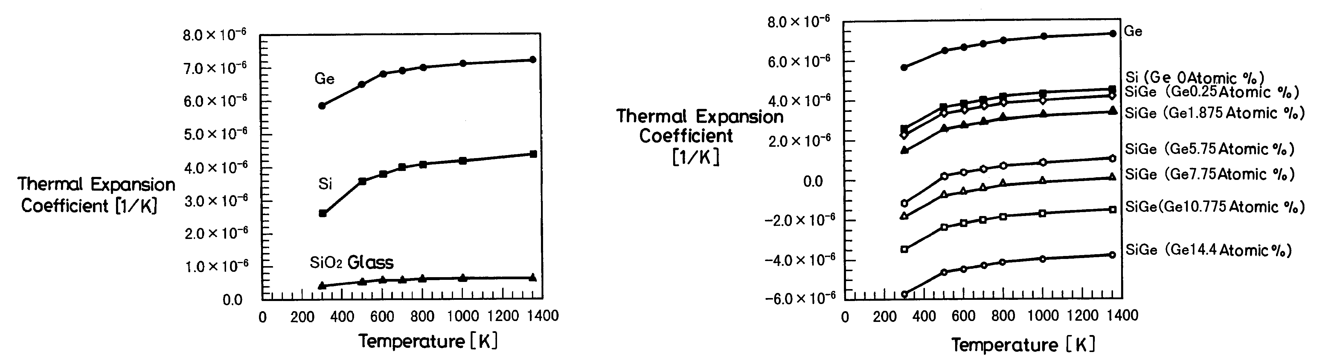
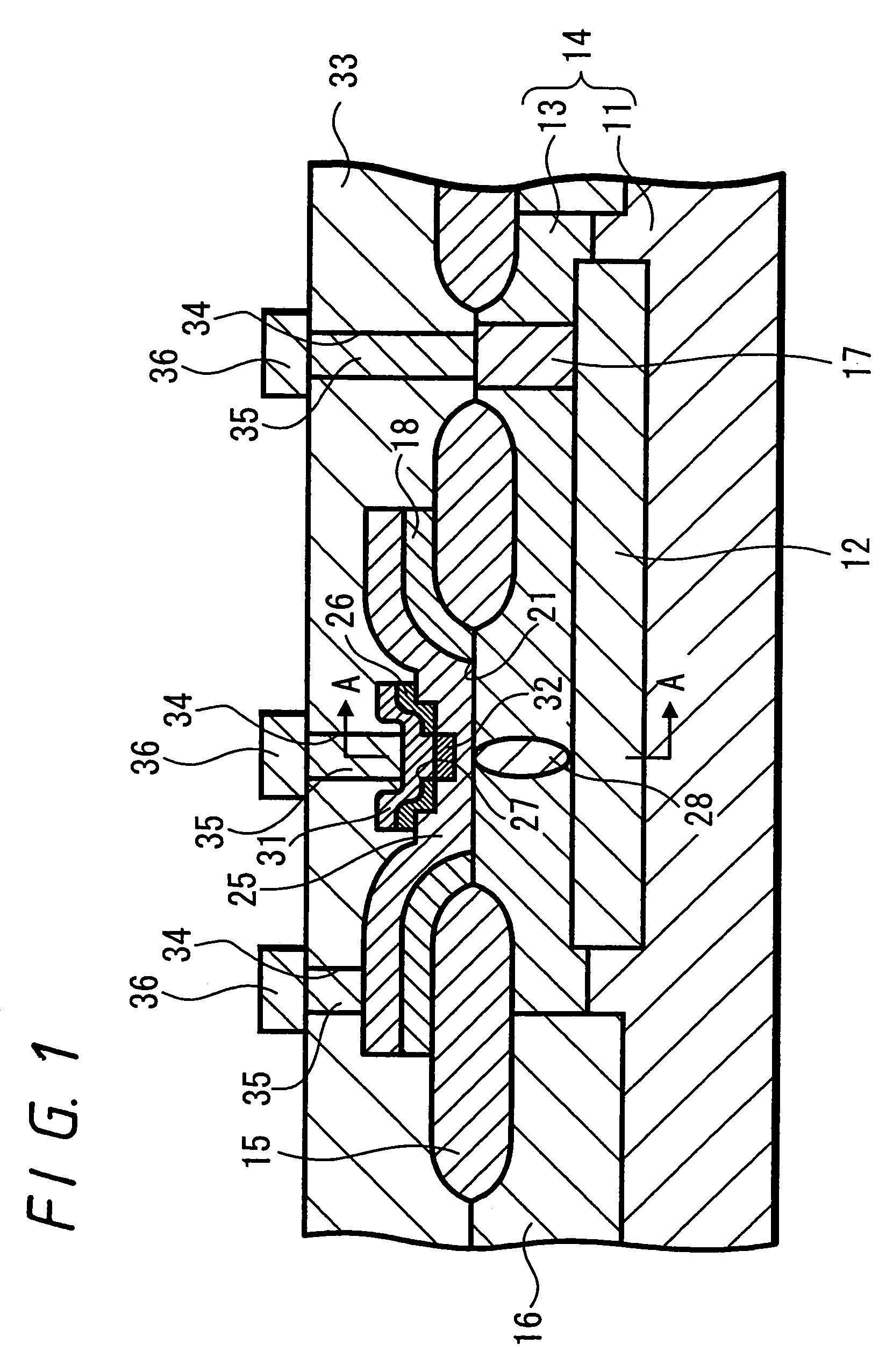
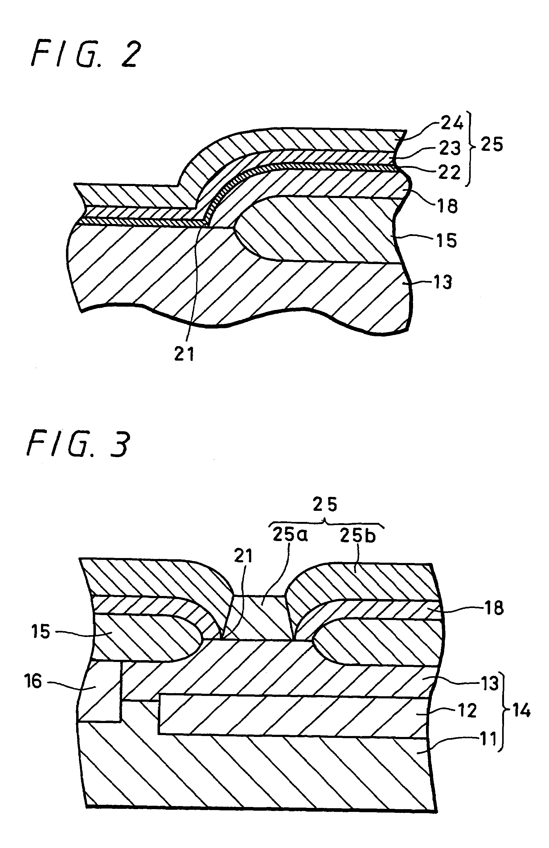
[0053]A first example refers to a manufacturing process of an SiGe hetero-junction bipolar transistor in which SiGe films that are communicating with each other are simultaneously formed on a single crystal Si substrate exposed through an opening of a silicon oxide (SiO2) film which prescribes a base forming region and the SiO2 film to form a single crystal SiGe film on the Si substrate as a base layer, a polycrystal SiGe film on the SiO2 film being formed as a base deriving electrode. In this case, since a stress caused by a difference among thermal expansion coefficients of Si, Ge and SiO2 also occurs in addition to a stress caused by a difference between the above-mentioned physical properties of Si and Ge, a misfit dislocation tend...


PUM

PropertyMeasurementUnit
thicknessaaaaaaaaaa
thicknessaaaaaaaaaa
temperatureaaaaaaaaaa

Abstract

The present invention relates to a semiconductor layer applicable to a hetero-junction bipolar transistor, a forming method thereof, and a semiconductor device and a manufacturing method thereof, for example. The semiconductor layer and the forming method thereof according to the present invention includes a first SiGe film or SiGeC film containing Ge of which the concentration become equal to a thermal expansion coefficient of silicon oxide and a second SiGe film or SiGeC film formed on the first film. In a semiconductor device according to the present invention and a manufacturing method thereof, first and second layers are laminated on an oxide film having an opening, and the first layer has the substantially same thermal expansion coefficient as that of the oxide film and has a thermal expansion coefficient different from that of the second layer. Thus, a stress that is caused by a difference between the thermal expansion coefficients becomes difficult to occur in the laminated film, and hence the occurrence of misfit dislocation can be suppressed. Thus, the present invention is suitable as the application to a hetero-junction bipolar transistor.

Description

TECHNICAL FIELD[0001]The present invention relates to a semiconductor layer containing a silicon germanium (SiGe) film or a silicon germanium carbon (SiGeC) film and a forming method thereof and a semiconductor device and a manufacturing method thereof.BACKGROUND OF THE INVENTION[0002]In recent years, in accordance with the arrival of a multimedia era in which information, services, entertainment, communications and the like are united, need for transmitting data of a large data amount at a high speed is progressively increasing, and it is also requested that bipolar transistors can operate at a higher speed. In order to enable the bipolar transistor to operate at a higher speed, a width of a base layer has to decrease and its carrier concentration has to increase. However, when a base layer is formed by implanting ions of impurities, due to channeling of impurities caused when ions of impurities are implanted, it is difficult to realize the base width of less than 40 nm. Therefore,...

Claims


Application Information

Patent Timeline
Patent Type & Authority Patents(United States)
IPC IPC(8): H01L21/331H01L29/737
CPCH01L29/66242H01L29/7378Y10S438/933Y10S438/938
Inventor KOUMOTO, TAKEYOSHIYAMAGATA, HIDEO
Owner SONY CORP
Why Eureka
Try Eureka