High-density plasma processing apparatus

A plasma and processing equipment technology, which is applied in the field of plasma processing equipment, can solve problems such as difficulty in maintaining the uniformity of wafer plasma distribution, and difficulty in distribution

Inactive Publication Date: 2005-02-02
SAMSUNG ELECTRONICS CO LTD
View PDF1 Cites 26 Cited by
  • Summary
  • Abstract
  • Description
  • Claims
  • Application Information

AI Technical Summary

Problems solved by technology

However, since the voltage applied to the ICP antenna increases as the ICP antenna increases, there is a limit to enlarging the ICP antenna
In addition, for plasma processing equipment using microwaves, it is difficult to transmit the high power of microwaves into the processing chamber without a significant increase in the size of the microwave source, and it is also difficult to uniformly distribute the microwave power into the processing chamber
[0012] As mentioned above, conventional plasma processing equipment cannot properly handle variations in process conditions due to the aforementioned problems, and thus cannot provide high plasma density and uniform distribution of plasma
In particular, with the recent trend towards larger wafers, it is more difficult for conventional plasma processing equipment to maintain uniformity of plasma distribution near the wafer
This significantly deteriorates the quality or yield of semiconductor devices

Method used


Image

  • High-density plasma processing apparatus
  • High-density plasma processing apparatus
  • High-density plasma processing apparatus

Examples


Embodiment Construction

[0027] The present invention will now be described more fully with reference to the accompanying drawings, in which preferred embodiments of the invention are shown. The embodiments of the present invention are intended to more fully explain the present invention to those skilled in the art. In the drawings, the same reference numerals denote the same elements.

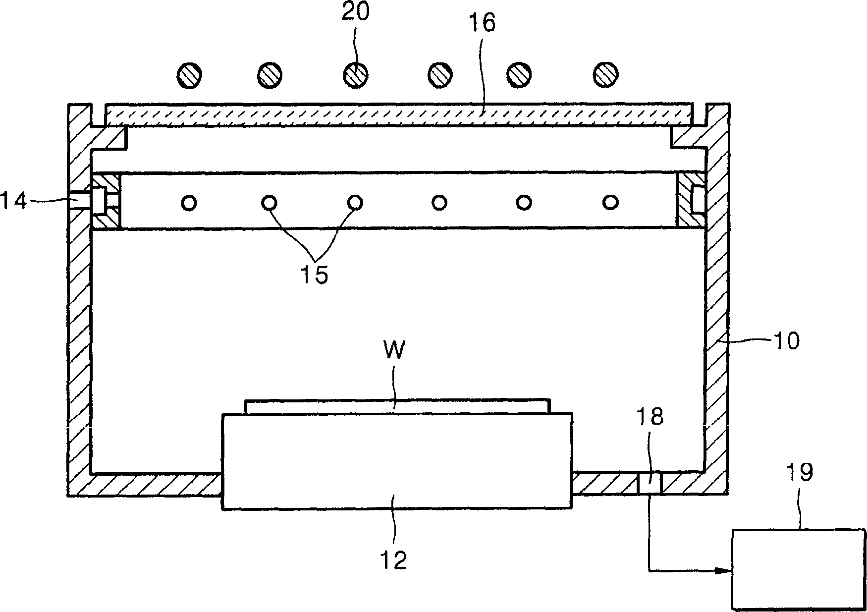
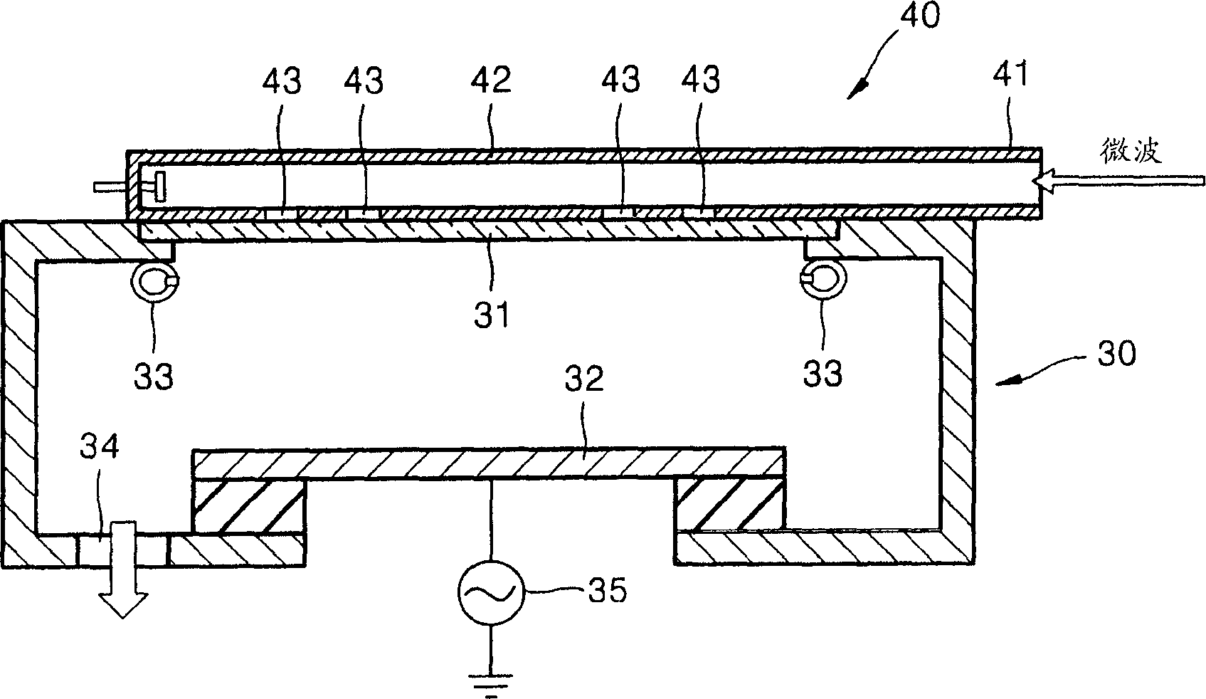
[0028] Figure 4 and Figure 5 are a vertical sectional view and a plan view showing the structure of the high-density plasma processing apparatus according to the first embodiment of the present invention, respectively. Please refer to Figure 4 and Figure 5 , the high-density plasma processing equipment of the present invention is a semiconductor processing equipment for performing micro-processing of wafers, for example, by using plasma to etch the surface of a silicon wafer (W) for semiconductor devices or by using plasma on the surface of a silicon wafer W The process of depositing a layer of material on to...


PUM


Abstract

The invention provides a fabrication plant for high density plasma, which comprises a processing room, a reaction gas refiller, an inductively coupled plasma antenna, a wave guide and an annular transmitting tube. A susceptor used for supporting the objects for processing is arranged within the processing room. A dielectric window is arranged on the processing room. The reaction gas refiller injects the reaction gases into the processing room. The inductively coupled plasma (ICP) antenna is arranged on the dielectric window to be positioned in the center of the dielectric window, and transfers the radio-frequency power from a radio-frequency power supply into the processing room. The wave guide guides the microwave generated by a microwave oscillator. The annular transmitting tube is arranged on the dielectric window to surround the inductively coupled plasma antenna, connected with the wave guide, and radiates microwave into the processing room via a plurality of incisions formed in the soleplate of the annular transmitting tube.

Description

technical field [0001] The present invention relates to high density plasma processing equipment designed to improve the uniformity of plasma distribution near the surface of a substrate. Background technique [0002] Plasma application technology is widely used in the process of micromachining substrates for manufacturing semiconductor devices or flat panel display panels. In other words, plasma is widely used to etch the surface of a wafer used for manufacturing a semiconductor device or the surface of a substrate used for manufacturing a liquid crystal display or to deposit a predetermined material layer on a substrate or a wafer. Therefore, the development of plasma processing equipment suitable for wafer etching processes or processes for depositing layers on wafers has become a core element in the development of methods and equipment for manufacturing semiconductor devices or flat panel display panels. [0003] Various types of plasma processing equipment exist, among...

Claims


Application Information

Patent Timeline
Patent Type & Authority Applications(China)
IPC IPC(8): H05H1/46C23C16/00H01J37/32H01L21/00H01L21/205H01L21/3065H05H1/00
CPCH01J37/32211H01J37/321H01L21/205
Inventor 尤里·N·托尔马切夫瑟吉·Y·纳瓦拉马东俊金大一
Owner SAMSUNG ELECTRONICS CO LTD
Why Eureka
Try Eureka