Equipment and method for picking electronic component

A technology of electronic components and equipment, applied in the field of picking equipment, can solve problems such as difficult detection of optical systems

Inactive Publication Date: 2005-02-02
ISMECA SEMICONDUCTOR HOLDING SA
View PDF0 Cites 0 Cited by
  • Summary
  • Abstract
  • Description
  • Claims
  • Application Information

AI Technical Summary

Problems solved by technology

However, this approach is only partially satisfactory, since it does allow only the positions of at most two edges of each element to be accurately determined
It is quickly limited in the

Method used


Image

  • Equipment and method for picking electronic component
  • Equipment and method for picking electronic component
  • Equipment and method for picking electronic component

Examples


Embodiment Construction

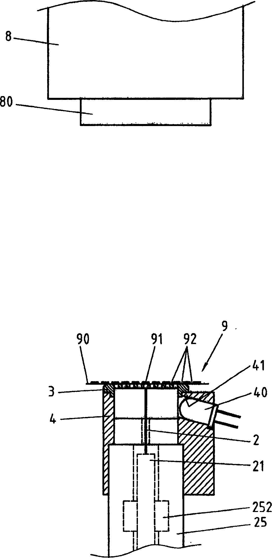
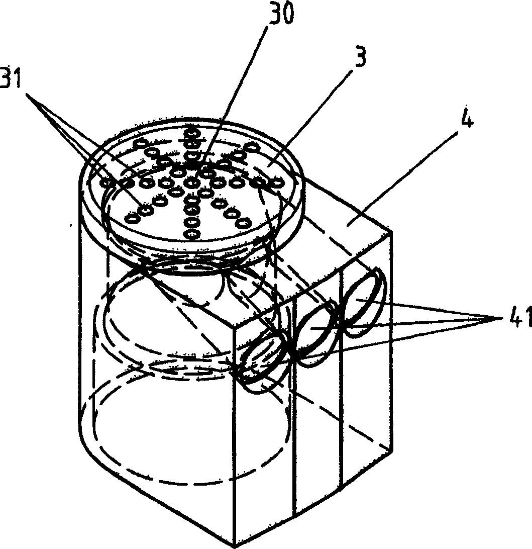
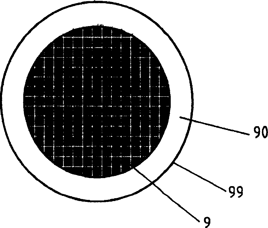
[0026] According to the preferred embodiment of the present invention, pick-up equipment is particularly suitable for from being bonded on the flexible film 90, then cut so that be divided into on the wafer 9 of individual element ( image 3 ) to extract electronic components, for example, electronic components such as LLP. The elastic membrane 90 is preferably stretched over the frame 99 to maximize the separation of the electronic components from each other.

[0027] Picking device of the present invention, in figure 1 The upper part is shown, comprising the needle 2, which is held approximately vertically, with its tip pointing upwards within a seat 25 (eg cylindrical). Needle 2 is movable along its longitudinal axis. Its base 21 slides preferably via bearings 252, which mounts keep it in a perfectly rectilinear trajectory. The movement of the needle 2 is driven by a motor (not shown), for example by a linear drive or by a rotary cylinder motor associated with a mechani...


PUM


Abstract

Equipment for picking electronic component (91) from dissected wafer (9) includes an optical device (8) which is allowed for screening the image of the first side of the dissected wafer (9); and a lighting unit (3, 40) for lighting the second side of the dissected wafer (9) facing the first side. A method for picking the electronic component (91) includes screening the first side of the electronic component (9) and lighting the second side of the electronic component (9) facing the first side. The back light irradiation of the electronic component (91) to be picked allows its boundary and its position to be determined by the optical device accurately.

Description

technical field [0001] The invention relates to a device for controlling the picking of electronic components, a device for picking electronic components comprising such a control device, and a method for determining the position and / or center of an electronic component. The invention relates in particular to an apparatus for controlling the extraction of electronic chips and / or packaged leadless components (leadless packages, LLPs) from a diced semiconductor wafer or from a diced "lead frame". The present invention also relates to a method of accurately determining the position and / or center of an electronic chip and / or a leadless component of a package (leadless package, LLP). Background technique [0002] Electronic chips and LLPs are often electronic components of very small size. Electronic chips are formed in series on a semiconductor wafer, which is generally circular and about 10 to 30 centimeters in diameter. LLPs are typically fabricated on rectangular wafers kno...

Claims


Application Information

Patent Timeline
IPC IPC(8): H01L21/00H05K13/00
Inventor P·罗伊T·埃米P·德罗马尔
Owner ISMECA SEMICONDUCTOR HOLDING SA
Why Eureka
Try Eureka