Thin film transistor, active matrix substrate, display device and electronic equipment

A technology of thin film transistors and display devices, applied in the direction of transistors, circuits, electrical components, etc., can solve problems such as difficulty in ensuring reliability, reduction in retention characteristics, reduction in liquid crystal capacitance and pixel area, etc., to achieve high reliability and ensure reliability , The effect of reducing the number of wiring

Inactive Publication Date: 2005-02-09
SEIKO EPSON CORP
View PDF1 Cites 8 Cited by
  • Summary
  • Abstract
  • Description
  • Claims
  • Application Information

AI Technical Summary

Problems solved by technology

However, in an ultra-high-definition display device, the liquid crystal capacitance decreases proportionally to the area of ​​the pixel, thereby significantly reducing the retention characteristics. Therefore, it is difficult to suppress the above-mentioned reduction in the retention characteristics only by the effect of reducing the off-state current of the LDD structure.
[0007] In addition, in a thin film transistor with a compensation structure, it is possible to obtain an off-state current characteristic superior to that of a thin film transistor with an LDD structure, but the characteristic degradation due to hot carriers is significant, and it is difficult to ensure reliability.

Method used


Image

  • Thin  film transistor, active matrix substrate, display device and electronic equipment
  • Thin  film transistor, active matrix substrate, display device and electronic equipment
  • Thin  film transistor, active matrix substrate, display device and electronic equipment

Examples


Embodiment 1

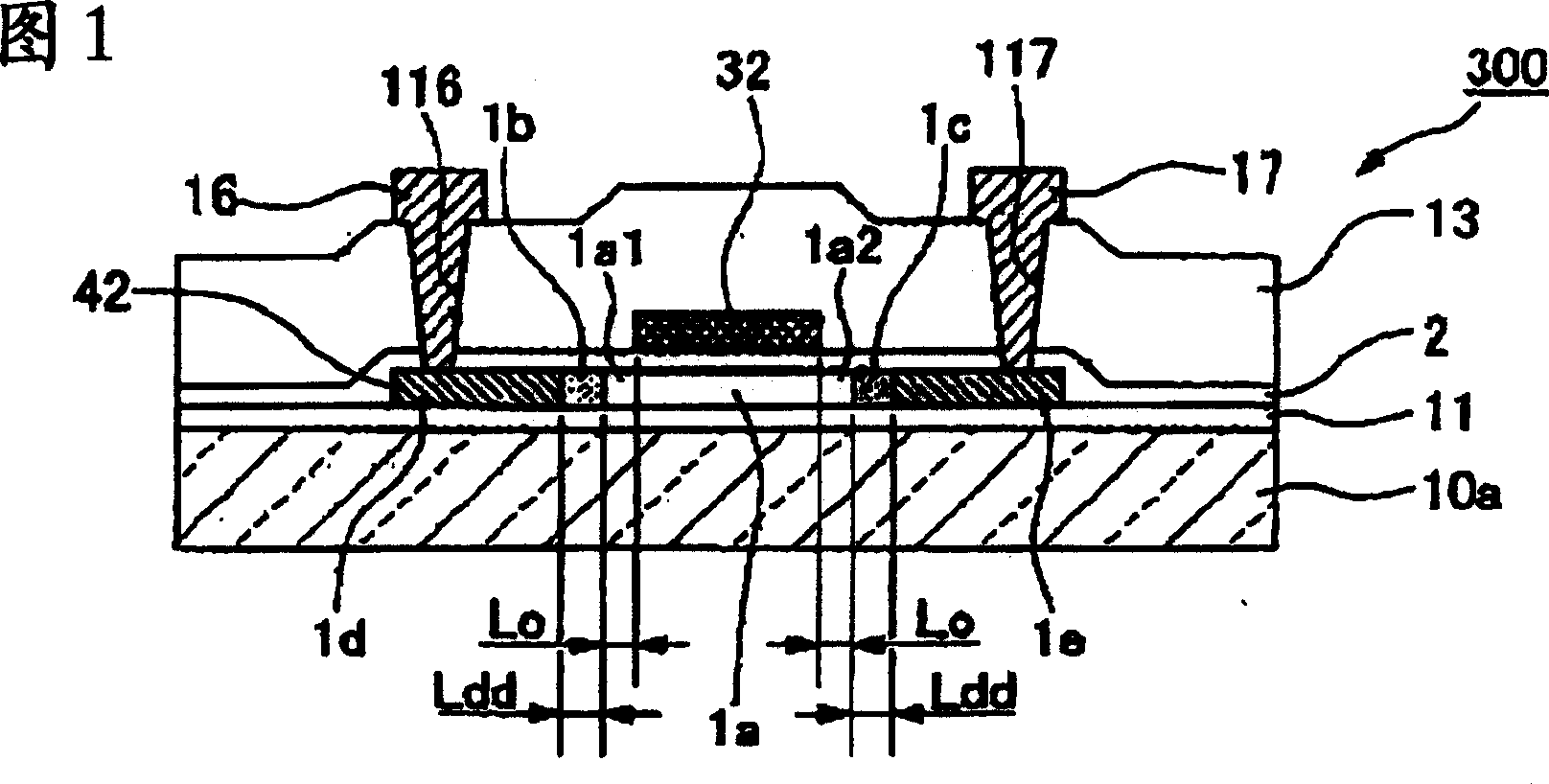
[0054] FIG. 1 is a cross-sectional view showing a first embodiment of the thin film transistor of the present invention. The TFT 300 shown in FIG. 1 is composed of a semiconductor layer 42 made of polysilicon formed on a substrate main body 10a made of an insulating material such as glass or quartz with an insulating base film 11 interposed therebetween, and an insulating film (gate electrode) formed to cover the semiconductor layer 42 . The insulating film) 2, the gate electrode 32, the source electrode 16, and the drain electrode 17 are mainly constituted.

[0055] The semiconductor layer 42 has a channel region 1a facing the gate electrode 32, compensation regions 1a1 and 1a2 connected to the channel region 1a, a low-concentration source region 1b and a low-concentration drain region 1c, a high-concentration source region 1d, and a low-concentration drain region 1c. High-concentration drain region 1e.

[0056] The above-mentioned channel region 1a and compensation region 1...

Embodiment 2

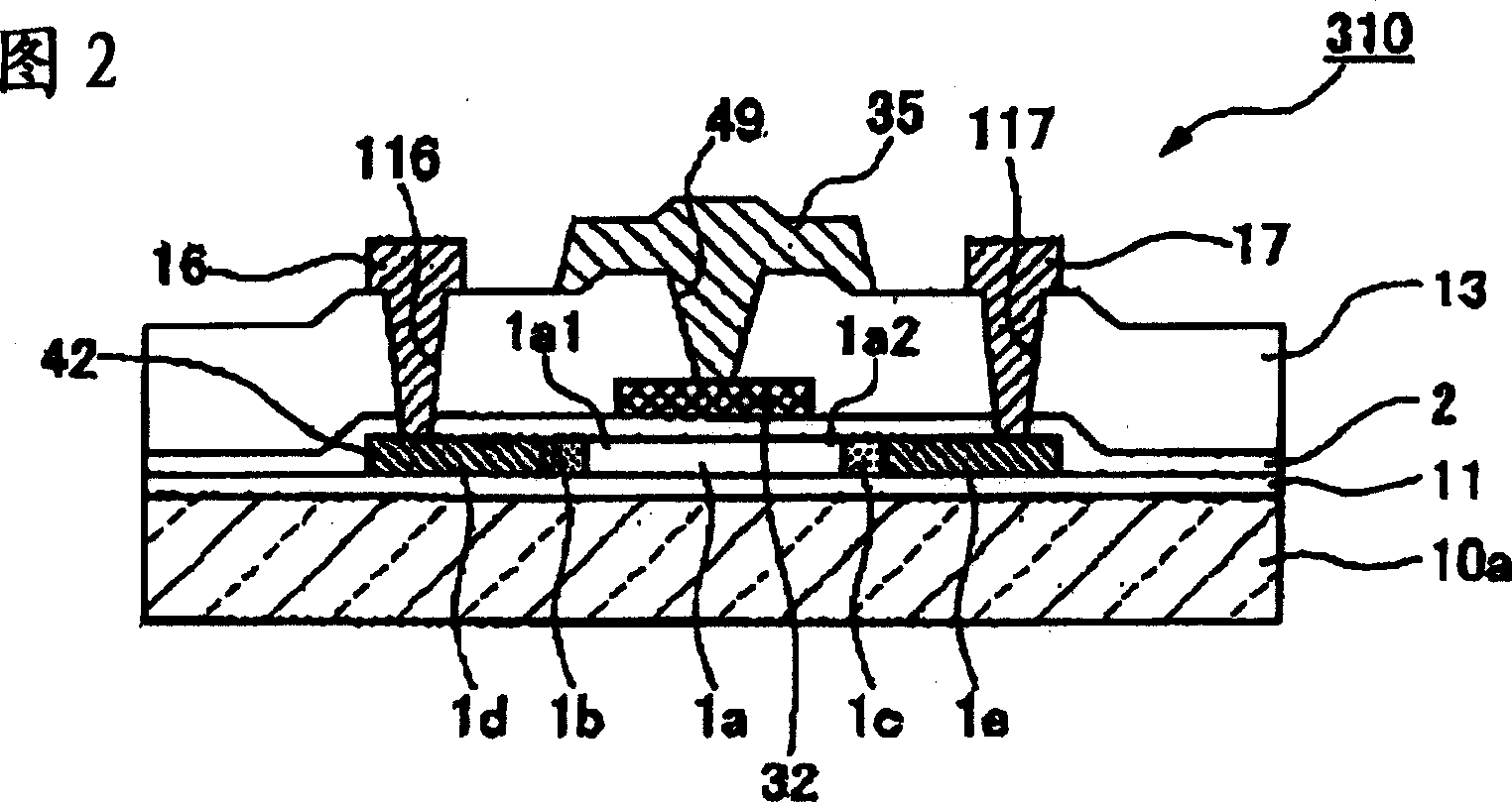
[0069] Fig. 2 is a cross-sectional view showing a second embodiment of the thin film transistor of the present invention. TFT (Thin Film Transistor) 310 shown in FIG. 2 has a structure in which wing-shaped gate electrode (second gate electrode) 35 having a substantially T-shaped cross section electrically connected to gate electrode 32 is provided relative to TFT 300 shown in FIG. 1 . Such a wing-shaped gate electrode 35 is formed to cover the gate electrode 32 on the semiconductor layer 42 and the compensation regions 1a1 and 1a2 of the semiconductor layer 42 in plan view. In this embodiment, the left-right direction of the wing-shaped gate electrode 35 is The edge ends are located in the planar regions of the low-concentration drain region 1 c and the low-concentration source region 1 b of the semiconductor layer 42 . Furthermore, the wing-shaped gate electrode 35 is electrically connected to the gate electrode 32 through a contact hole 49 provided through the first interlay...


PUM

PropertyMeasurementUnit
lengthaaaaaaaaaa
thicknessaaaaaaaaaa

Abstract

Provided is a thin film transistor which has an off-state current reduced to an extremely low level, and has an outstanding reliability, and is preferably applicable to a pixel driver of a super high definition indicator, peripheral circuits or the like, to provide an active matrix substrate provided with the thin film transistor, and to provide a display. Thin film transistor comprises a semiconductor layer 42 provided on a substrate main body 10a, a gate electrode 32, a drain electrode 17, and a source electrode 16. The semiconductor layer 42 is connected with the drain electrode 17. It is so constituted that there are provided a high concentration drain region 1e where impurity is heavily diffused, a low concentration drain region 1c provided at the gate electrode 32 side of the high concentration drain region 1e where the impurity is lightly diffused, and a region provided at the gate electrode 32 side of the low concentration drain region 1c where the impurity is diffused in a minute amount concentration, or alternatively an offset region 1a2 set as an intrinsic semiconductor region.

Description

technical field [0001] The invention relates to thin film transistors, active matrix substrates, display devices and electronic equipment. Background technique [0002] In the field of display devices including liquid crystal devices, there is an increasing demand for higher brightness and higher definition. For example, digitalization of photographs is now progressing. image display device. However, current technology cannot yet realize such an ultra-high-definition display device. The main reason for this is that the off-state current of transistors used in pixels cannot be reduced. [0003] Conventionally, the semiconductor layer of a thin film transistor of a liquid crystal device is formed from amorphous silicon (amorphous silicon), a method of forming a low-temperature polysilicon film, or a method of forming a high-temperature polysilicon film. The method of manufacturing with a low-temperature polysilicon film has the advantages of being able to form an image sign...

Claims


Application Information

Patent Timeline
Patent Type & Authority Applications(China)
IPC IPC(8): G02F1/1368G02F1/136H01L21/336H01L27/12H01L29/78H01L29/786
CPCH01L29/66757H01L29/78621H01L27/12H01L2029/7863G02F1/136
Inventor 小出慎
Owner SEIKO EPSON CORP
Why Eureka
Try Eureka