
Circuit board transferring apparatus and method and solder ball mounting method

一种电路基板、搬运装置的技术,应用在电路、送锡装置、辅助装置等方向,能够解决焊球吸附管嘴排列不一致、焊盘精度差、无法焊球准确地搭载搭载等问题

Inactive Publication Date: 2005-05-18
NIIGATA SEIMITSU
View PDF4 Cites 4 Cited by
  • Summary
  • Abstract
  • Description
  • Claims
  • Application Information

AI Technical Summary

Problems solved by technology

Therefore, even if a plurality of CSPs 52 are arranged by shape recognition, the pads contained in the plurality of CSPs 52 may not always be arranged in the correct position, and thus there is a problem that the accuracy of the position matching of the pads is poor.
[0018] For example, if Image 6 As shown, when the three CSPs 52 that are not arranged in the same position are recognized according to the appearance, although the CSPs 52 themselves are correctly arranged at equal intervals, the important pads 57 as a whole and is not aligned exactly so that it does not coincide with the alignment of the solder ball pickup nozzle
Therefore, there is a case where the solder ball cannot be accurately mounted on each pad, and the mounting failure occurs.

Method used


Image

  • Circuit board transferring apparatus and method and solder ball mounting method
  • Circuit board transferring apparatus and method and solder ball mounting method
  • Circuit board transferring apparatus and method and solder ball mounting method

Examples


Embodiment Construction

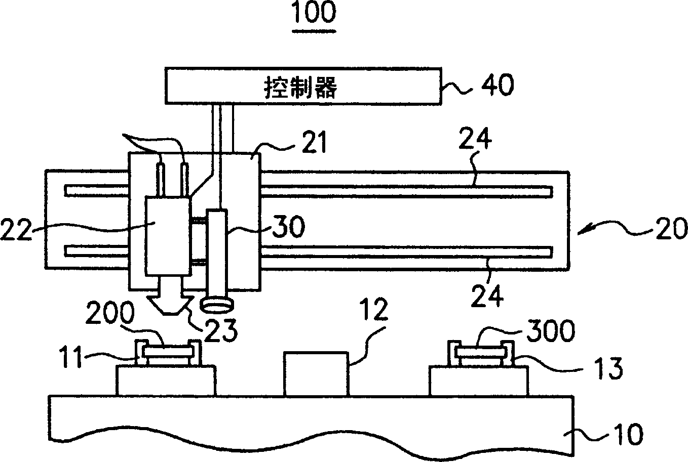
[0032] An embodiment of the present invention will be described below with reference to the accompanying drawings. figure 1 It is a figure which shows the schematic structure example of the circuit board conveyance apparatus of this embodiment. Such as figure 1 As shown, the circuit board transfer device 100 of this embodiment has a base 10 , a moving mechanism 20 , a camera 30 , and a controller 40 .

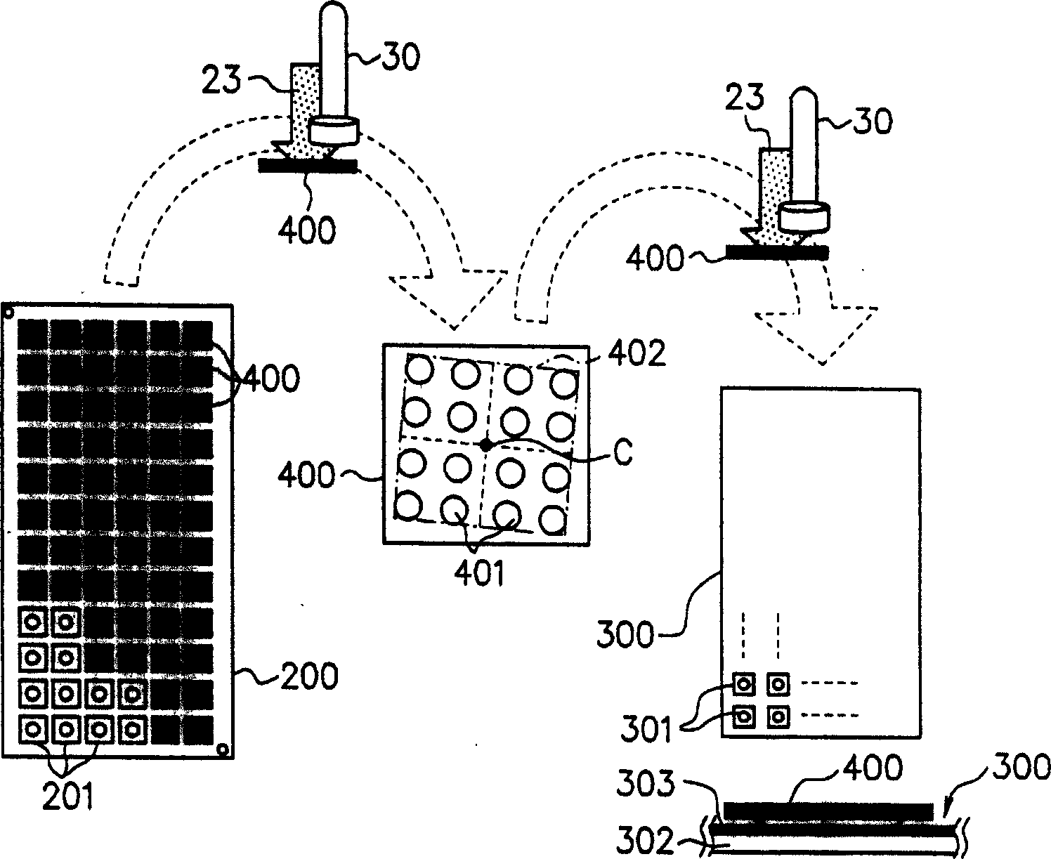
[0033] On the base 10, a tray support 11, an imaging stand 12, and a carrier support 13 are provided. The tray holder 11 is a member that holds a dedicated tray 200 for placing a plurality of circuit boards (for example, CSP) of a BGA structure semiconductor package before mounting solder balls. On the BGA tray 200 , grid-shaped CSP storage portions are formed at substantially equal intervals, and a plurality of CSPs are placed on each CSP storage portion with the pad formation surface facing upward.

[0034] The imaging stage 12 is a stage for placing the CSP picked up fr...


PUM


Abstract

The present invention provides a conveying device, a conveying method, and a solder ball mounting method for a circuit board. By photographing the pad formation surface of a CSP (400) and identifying the pad arrangement by image processing, CSP is performed based on the recognition result of the pad arrangement. (400) transport positioning, even if the pads (401) are formed in any arrangement state in the CSP (400) to be transported, the positional relationship of a plurality of pads (401) contained in each CSP (400) can be made The positional relationship with the plurality of solder ball suction nozzles included in the solder ball mounting device is always exactly the same. Thereby, when solder balls are mounted on a plurality of BGAs at once, it is possible to prevent solder ball mounting defects from occurring.

Description

technical field [0001] The present invention relates to a conveyance device, a conveyance method, and a solder ball mounting method of a circuit board, and relates to a device for conveying, for example, a circuit board of a plurality of BGA semiconductor modules before being mounted with solder balls on a pallet in a row and after being conveyed to the pallet. A method of mounting solder balls on a circuit board of a BGA semiconductor component. Background technique [0002] In recent years, the internal circuits of semiconductor devices used in electronic equipment have become more complex, and the number of signals exchanged with the outside has gradually increased in response to the demand for higher functionality and smaller and lighter electronic equipment. In this way, the miniaturization and multiple pins of semiconductor components are gradually improved. As a high-density packaging technology corresponding to the miniaturization and multi-pin increase of such a se...

Claims


Application Information

Patent Timeline
Patent Type & Authority Applications(China)
IPC IPC(8): H05K3/34B23K3/06H01L23/12
CPCB23K3/0607H05K3/3478H01L2224/13B23K2101/42
Inventor 间野昭浩上野幸宏浦泽裕德田中昭广
Owner NIIGATA SEIMITSU
Learn More