Method for preparing field effect transistor

A field effect transistor and process method technology are applied in the field of preparation of quasi-SOI field effect transistors, and can solve the problems of complex preparation process, high preparation cost, limitation of quasi-SOI application, and the like

Active Publication Date: 2005-06-01
PEKING UNIV +1
View PDF0 Cites 16 Cited by
  • Summary
  • Abstract
  • Description
  • Claims
  • Application Information

AI Technical Summary

Problems solved by technology

These processes usually require specific equipment, the preparation process is relatively complicated, the preparation cost is relatively high, and it is not compatible with the traditional CMOS process, which greatly limits the application of quasi-SOI in integrated circuits

Method used


Image

  • Method for preparing field effect transistor
  • Method for preparing field effect transistor
  • Method for preparing field effect transistor

Examples


Embodiment Construction

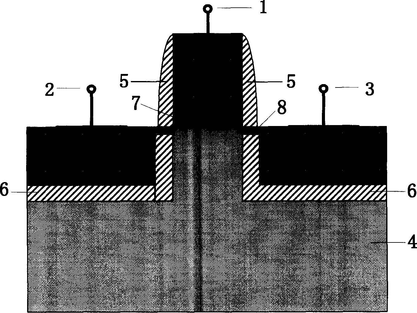
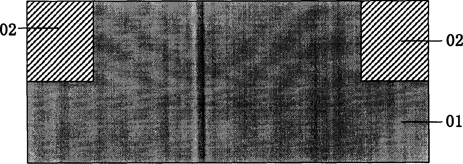
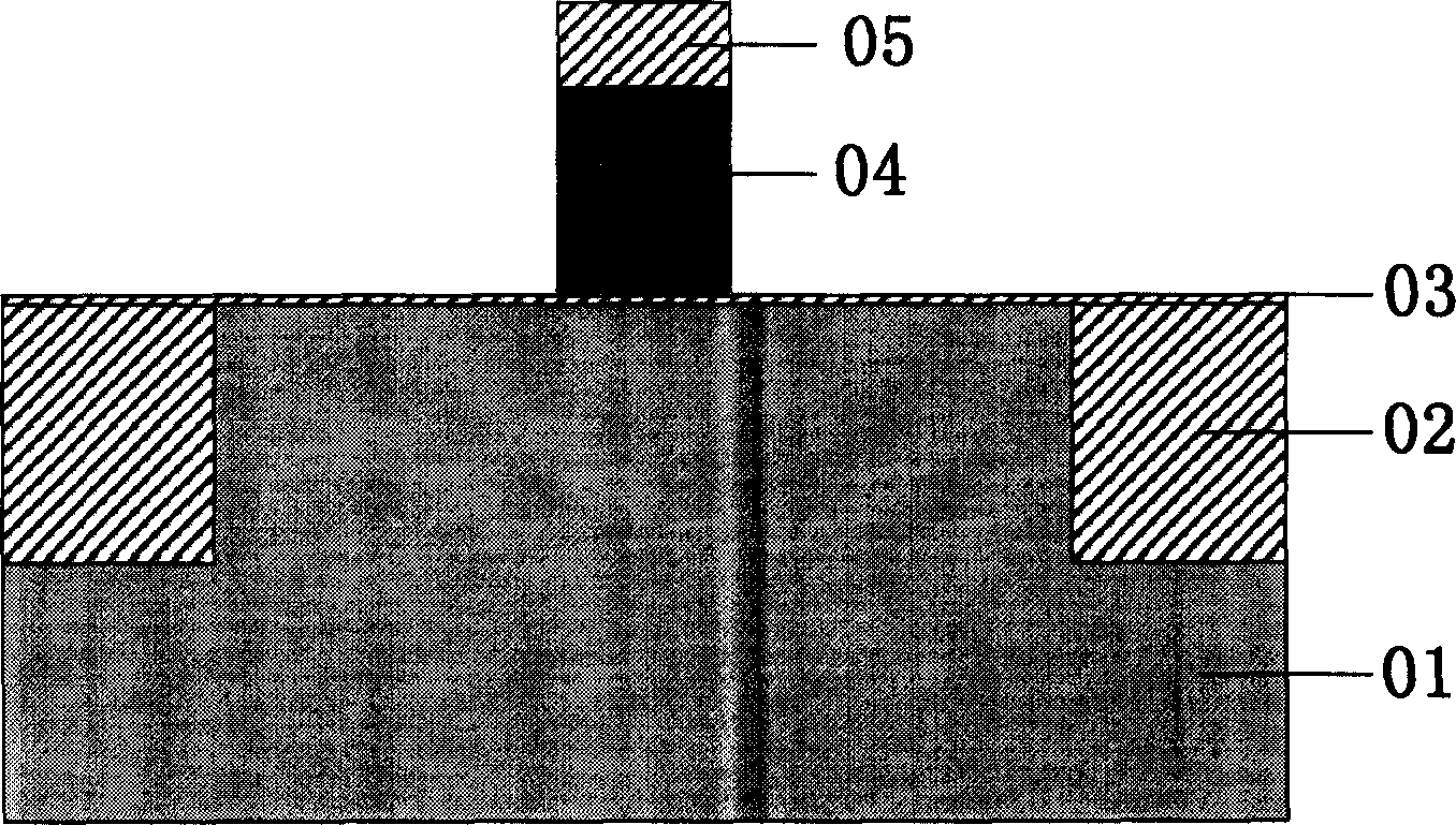
[0023] In the invention, the gate region and the channel region below it are firstly defined, and then the source and drain regions are formed. The specific method is as follows: the first step is to use a conventional process method to realize shallow trench isolation, deposit and etch the gate material and the hard mask material covering it to form the gate region, and then prepare the gate sidewall to protect the gate region. The wall thickness is L1. The second step is to form an oxide layer. First, etch the silicon in the source and drain regions to a certain depth h1, then deposit and etch anti-oxidation materials to form side walls with a width of L2, and then further etch the silicon material in the source and drain regions To the second depth h2, a deeper silicon groove is formed, and finally the exposed silicon is thermally oxidized to obtain an "L"-shaped silicon oxide with a thickness of L3. In order to ensure that the channel region is directly connected to the su...


PUM


Abstract

The present invention provides the preparation process of quasi-SOI FET, and belongs to the field of ULSI technology. The preparation process includes the first conventional technological step of shallow channel isolation, depositing and etching grid material and covered hard mask material to form grid area, and forming grid side wall to protect grid area; the second step of etching silicon in source and drain areas to certain depth h1, depositing and etching antioxidant material to form side wall, etching silicon in source and drain areas to the second depth h2 to form deeper silicon channel, and hot oxidizing the exposed silicon to form L-shaped silica layer inside the channels in source and drain areas; and the third step of eliminating side wall of antioxidant material, depositing source and drain material and forming source arean and drain arean in flat course, so as to form the quasi-SOI structure. The said process is simple, low in cost and easy in integration.

Description

technical field [0001] The invention belongs to the field of ultra-large-scale integrated circuit technology (ULSI), in particular to a preparation method of a quasi-SOI field-effect transistor. Background technique [0002] With the development of microelectronics technology, the feature size of devices has entered the deep submicron (<0.1um) range. At this time, the field effect transistors prepared by the traditional CMOS bulk silicon technology are greatly limited in application due to the severe short channel effect and other parasitic effects. The use of SOI (silicon on insulator) technology, especially fully depleted SOI devices, can well suppress the short-channel effect, obtain small threshold voltage fluctuations and near-ideal sub-threshold slopes; at the same time, the devices are fabricated on SiO 2 On the other hand, the parasitic junction capacitance can be reduced, thereby increasing the speed of the device. However, SOI devices are limited by the proble...

Claims


Application Information

Patent Timeline
Patent Type & Authority Applications(China)
IPC IPC(8): H01L21/335
Inventor 肖韩黄如田豫
Owner PEKING UNIV
Why Eureka
Try Eureka