Micro flow control chip with integrated dialysis function and preparing process thereof

A microfluidic chip and functional technology, which is applied in the preparation of test samples, analytical materials, instruments, etc., can solve the problems of solution flow range flow range mismatch, complex processing and operation technology, etc.

Inactive Publication Date: 2005-06-22
DALIAN INST OF CHEM PHYSICS CHINESE ACAD OF SCI
View PDF0 Cites 26 Cited by
  • Summary
  • Abstract
  • Description
  • Claims
  • Application Information

AI Technical Summary

Problems solved by technology

The processing and operation technology of the former is complicated, and the solution flow range of the commercial microdialysis tube does not match the flow range of the conventional microfluidic chip; the latter is sealed by mechanical pressure, and it is difficult to integrate other functional units on the chip

Method used


Image

  • Micro flow control chip with integrated dialysis function and preparing process thereof

Examples


Embodiment Construction

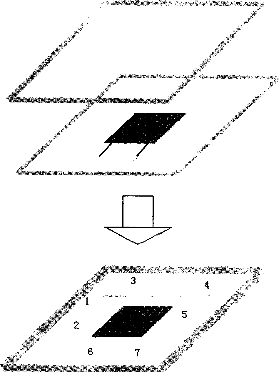
[0018] exist figure 1 In the chip design shown, two functional units of dialysis pretreatment and electrophoretic separation are integrated on the same chip. The main body of the chip is composed of upper and lower layers of PDMS, the solid line represents the lower channel, and the dotted line represents the upper channel; the shaded part is the dialysis membrane, which is sandwiched between the two layers of PDMS chips to separate the upper and lower channels. The specific processing process is as follows:

[0019] 1. Use SU-8 photoresist on the surface of the silicon wafer (or glass wafer) to make protrusions with upper and lower layer channel shapes respectively, as a template for pouring the upper and lower layer PDMS chips.

[0020] 2. Pour about 5mm thick PDMS (5:1) on the upper template, and pour about 2mm thick PDMS (20:1) on the lower template, and put both into an oven at 80°C for polymerization About 30 minutes.

[0021] 3. After peeling off from the template, p...


PUM

PropertyMeasurementUnit
thicknessaaaaaaaaaa
thicknessaaaaaaaaaa

Abstract

This invention provides a micro flow control chip formed by three sealed parts integrating the dialyzing functions. The top and bottom layers of the chip have channels for microfluid and the sandwich layer is a dialysis membrane. The preparation method includes three steps: first of all, casting the upper and lower PDMS layer to be aggregated in a bake oven for 20-60min to be stripped from the form board, a small hole on the top is opened for the fluid enter then the dialysis membrane is stuck at a suitable place of the bottom PDMS to be adhered closely with the top to align the two layers of channels accurately, finally, the total chip is aggregated for 1~3h in a bake oven, the chip is always sealed.

Description

Technical field: [0001] The invention relates to a functionalized microfluidic chip processing technology, and in particular provides a new technology for integrating a dialysis function on a microfluidic chip. Background technique: [0002] Recent developments show that lab-on-a-chip technology will play a similar role in promoting the development of analytical science and even the entire science and technology in the next ten to twenty years as microelectronics technology played in the development of information science forty years ago. The so-called lab-on-a-chip refers to the integration or basic integration of basic operating units such as sample preparation, biological and chemical reactions, separation, and detection involved in the fields of biology and chemistry into a chip of a few square centimeters to complete different tasks. A technique for analyzing the process of a biological or chemical reaction and analyzing its products. At present, the development of the...

Claims


Application Information

Patent Timeline
Patent Type & Authority Applications(China)
IPC IPC(8): G01N1/28G01N35/00
Inventor 龙志成林炳承
Owner DALIAN INST OF CHEM PHYSICS CHINESE ACAD OF SCI
Why Eureka
Try Eureka