USB application apparatus

An application module and corresponding technology, applied in coupling devices, two-part connection devices, electrical components, etc., can solve problems such as work efficiency and functional limitations, waste, insufficient data transmission lines, etc., and achieve improved signal transmission bandwidth and transmission Speed, increased work efficiency and functionality, reduced overall size

An application module and corresponding technology, applied in coupling devices, two-part connection devices, electrical components, etc., can solve problems such as work efficiency and functional limitations, waste, insufficient data transmission lines, etc., and achieve improved signal transmission bandwidth and transmission Speed, increased work efficiency and functionality, reduced overall size

CN1632987AInactive Publication Date: 2005-06-29INNODISK CORP

Image

  • USB application apparatus
  • USB application apparatus
  • USB application apparatus

Examples


Embodiment Construction

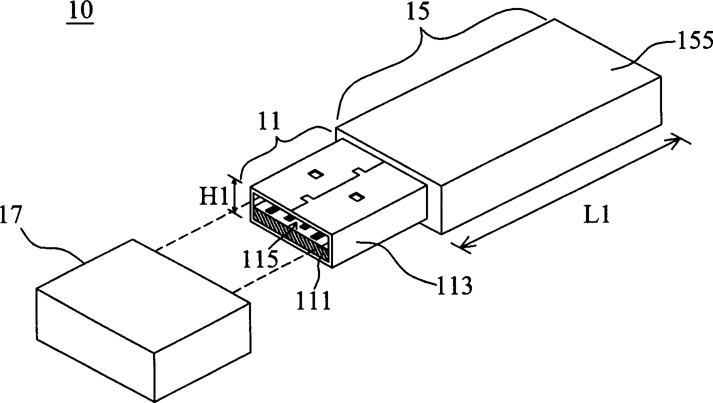
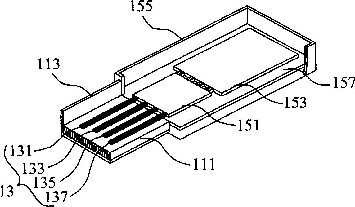
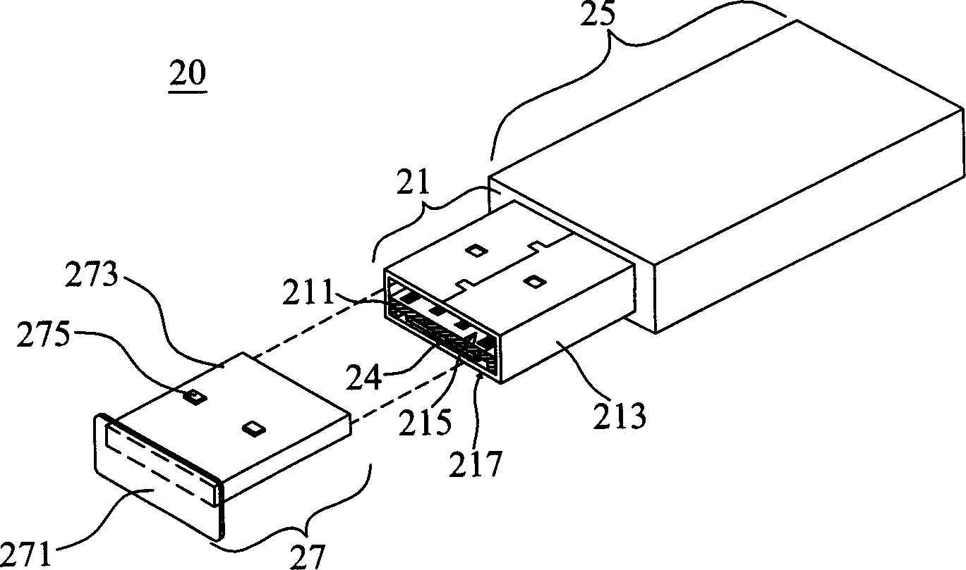
[0065] Such as image 3 and Figure 3A As shown, the USB application device 20 of the present invention, such as mobile hard disk, Bluetooth, digital camera, MP3 player, control circuit, GPS, recording pen, TV viewing module or wireless network card module and other devices, its front end is provided with a connector (Series A Plug) 21, the rear end of the connector 21 is connected with a USB electronic application module 25. Wherein, the shell layer 213 of the connector 21 encloses a PCB carrier board 211 made of a PCB circuit board, and a connecting interlayer 215 can be naturally formed between the top surface of the PCB carrier board 211 and the outer shell layer 213, the connecting interlayer 215 can be plugged with another connection socket (Series A receptacle), and the top surface of the PCB carrier board 211 in the connection interlayer 215 can carry a plurality of first connection terminals 23 electrically connected to the electronic application module 25 . When th...


PUM


Abstract

This invention discloses a USB applied device taking a PCB as the carrier board of a connector, the top surface of the carrier board can load multiple first connecting terminals and its bottom interlayer is formed between the bottom surface of PCB carrier board and the shell layer of the connector, for fixing an electronic component to reduce the length of the USB module or increase its working efficiency and function, besides, a data transmission circuit is set on part of the top surface without the first connection end on the PCB carrier board to increase its working efficiency and function.

Description

technical field [0001] The present invention relates to a USB application device, in particular to an improved structure using a PCB circuit board as an internal bearing board of a connector, which can not only reduce the length of the USB application device, but also effectively improve the working efficiency and functions of the USB application device . Background technique [0002] The USB (Universal Serial Bus) transmission interface is widely used in various computer peripheral devices, information appliances (IA) or 3C consumer electronics products due to its advantages of convenience, expandability and high transmission speed. , is an indispensable transmission interface tool in people's work and family life today. [0003] The existing USB device terminal structure is as follows: figure 1 and figure 2 As shown, a USB application device 10 with a USB connector 11 (Series A Plug), such as an MP3 player or a recorder, etc., has a USB connector 11 at its front end, a...

Claims


Application Information

Patent Timeline
29 Jun 2005
Publication
CN1632987A
IPC
H01R12/00; H01R24/66
Inventors
李钟亮; 林传生