Detecting method and structure for microstructure binding process

A bonding process and detection method technology, applied in the direction of measuring devices, instruments, surface/boundary effects, etc., can solve the problem that the bonding sample cannot be too small, cannot accurately reflect the bonding strength of the microstructure, and cannot reflect the bonding strength Influence and other issues, to achieve the effect of improving the yield of MEMS device processing, convenient detection, and simple process

A bonding process and detection method technology, applied in the direction of measuring devices, instruments, surface/boundary effects, etc., can solve the problem that the bonding sample cannot be too small, cannot accurately reflect the bonding strength of the microstructure, and cannot reflect the bonding strength Influence and other issues, to achieve the effect of improving the yield of MEMS device processing, convenient detection, and simple process

CN1648634AInactive Publication Date: 2005-08-03PEKING UNIV

Image

  • Detecting method and structure for microstructure binding process
  • Detecting method and structure for microstructure binding process
  • Detecting method and structure for microstructure binding process

Examples


Embodiment Construction

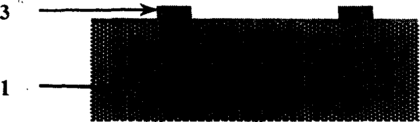
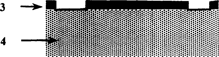
[0044] The present invention is mainly applicable to MEMS microstructures produced by the bonding strength detection of various microstructures using bonding techniques (for example: silicon-glass bonding, silicon ICP deep etching), and the present invention can also be used in other forms of bonding (such as silicon fusion bonding direct, adhesive bonding bonding, etc.) detection of microstructure bonding strength.

[0045] In this embodiment, the process of silicon-glass bonding and silicon ICP deep etching is specifically described, but it does not limit the application of the present invention to other bonding methods. The specific process flow is shown in the appendix Figure 1-7 and its description.

[0046] Silicon-glass bonding part:

[0047] In order to increase the bonding strength, necessary cleaning is performed on the bonding surfaces of the silicon structure wafer before the bonding alignment between the bonding surfaces is performed. Especially for silicon stru...


PUM


Abstract

The present invention relates to detection method and detection structure for micro structure bonding process result. The detection method includes first designing silicon structure pattern; preparing micro structure with silicon structure bonded with silicon substrate or glass substrate via bonding technological process, with the silicon structure having at least one end separated from the bonding surface and the bonding area being recorded; pushing the silicon structure on the no-bonding end with micro probe to make the silicon structure deform until the monocrystal silicon chip breaks from the bonding surface and recording the distance between the probe pushed point and the bonding surface, deformation and the breaking process parameters; and calculating the bonding strength based on the recorded data. The present invention completes MEMS device detection in a simple process.

Description

Technical field: [0001] The invention relates to the technical field of micro-electro-mechanical system (MEMS) processing technology, in particular to a detection method for microstructure bonding process results and a detection structure used in the method. Background technique: [0002] As an interdisciplinary and advanced manufacturing technology that originated in the 1990s, MEMS has played an important role in improving people's quality of life, improving people's living standards and enhancing national strength. Due to the strong interdisciplinary features, MEMS research methods and processing technologies are inherently diverse. Among many processing technologies, silicon technology is gradually becoming the mainstream of MEMS technology. Bonding, as a key technology in silicon technology, has been adopted more and more in recent years. [0003] "Bulk silicon MEMS device integration method" (CN1431699) discloses a bulk silicon MEMS device integration method, and its ...

Claims


Application Information

Patent Timeline
03 Aug 2005
Publication
CN1648634A
IPC
G01Q10/00
Inventors
阮勇; 张大成