Check patentability & draft patents in minutes with Patsnap Eureka AI!

Immersion lithography system, and method of performing irradiation to semiconductor structure having a photoresistive layer

An immersion lithography and photoresist layer technology, applied in the immersion lithography system and the field of immersion fluid, can solve the problem that the pH value is not further controlled, and achieve the effect of inhibiting pollution, inhibiting dissolution and reducing damage. Effect

Active Publication Date: 2005-08-17
TAIWAN SEMICON MFG CO LTD
View PDF4 Cites 5 Cited by
  • Summary
  • Abstract
  • Description
  • Claims
  • Application Information

AI Technical Summary

Problems solved by technology

[0014] The traditional immersion lithography technology uses water as the immersion fluid, but the pH value of water as the immersion fluid has not been further controlled

Method used


Image

  • Immersion lithography system, and method of performing irradiation to semiconductor structure having a photoresistive layer
  • Immersion lithography system, and method of performing irradiation to semiconductor structure having a photoresistive layer
  • Immersion lithography system, and method of performing irradiation to semiconductor structure having a photoresistive layer

Examples


Embodiment Construction

[0062] The following are preferred embodiments of the present invention to illustrate the immersion photolithography system and its usage according to the present invention.

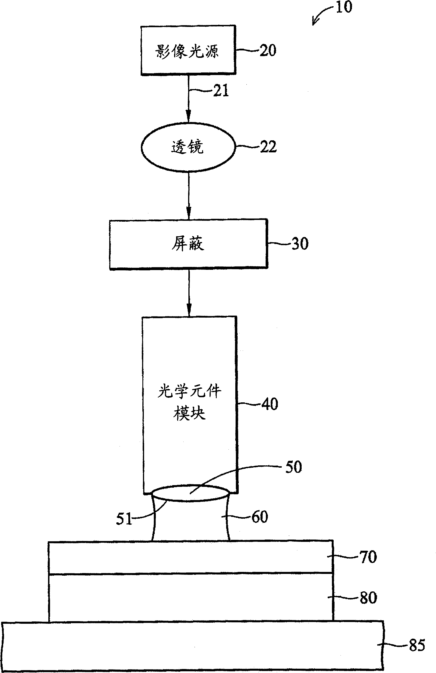
[0063] figure 1 is a schematic diagram of one embodiment of an immersion lithography system 10 . The immersion lithography system 10 includes an image light source 20, the light source 20 emits a light energy beam 21, and passes through a lens 22, then the light energy beam 21 passes through a shield 30 and an optical element module 40, and finally passes through a The outermost lens 50 of the optical surface 51 . The space between the outermost lens 50 and the photosensitive material 70 formed on the semiconductor element substrate 80 is filled with the immersion fluid 60 .

[0064] In a preferred embodiment, the semiconductor element substrate 80 may be a semiconductor substrate on which an integrated circuit is formed. For example, the semiconductor element substrate 80 may be a silicon substrate (...


PUM

PropertyMeasurementUnit
wavelengthaaaaaaaaaa
sizeaaaaaaaaaa

Abstract

An immersion lithographic system 10 comprises an optical surface 51, an immersion fluid 60 contacting at least a portion of the optical surface, and a semiconductor structure 80 having a topmost photoresist layer 70 having a thickness of less than about 5000 angstroms, wherein a portion of the photoresist is in contact with the immersion fluid. Further, a method for illuminating a semiconductor structure 80 having a topmost photoresist layer 70 with a thickness of less than about 5000 angstroms, comprising introducing an immersion fluid 60 into a space between an optical surface 51 and the photoresist layer, and directing light preferably with a wavelength of less than about 450 nm through the immersion fluid and onto the photoresist.

Description

technical field [0001] The invention relates to a manufacturing process of a semiconductor element, in particular to a system and a method of an immersion photolithography technology and an immersion fluid used therein. Background technique [0002] In a typical photolithography system, in order to distinguish high-resolution patterns such as dots, lines or images, the photolithography system must have high resolution. In photolithography systems used in the integrated circuit (IC) industry, light is typically projected directly onto a photoresist layer to pattern electrode elements. Lithography systems have been used in the IC industry for decades and are expected to address processes below 50nm line width. Therefore, improving the resolution of the lithography system has become one of the most important issues for semiconductor IC chip manufacturers to manufacture high-density, high-speed semiconductor IC chips. [0003] For a photolithography system, its resolution R is...

Claims


Application Information

Patent Timeline
Patent Type & Authority Applications(China)
IPC IPC(8): G03F7/20H01L21/00H01L21/027
Inventor 杨育佳林本坚胡正明
Owner TAIWAN SEMICON MFG CO LTD
Features
  • R&D
  • Intellectual Property
  • Life Sciences
  • Materials
  • Tech Scout
  • Unparalleled Data Quality
  • Higher Quality Content
  • 60% Fewer Hallucinations
Learn More