Base plate processing device,base plate processing method and progarm

A technology for a substrate processing device and a substrate processing method, which is applied in the direction of electrical program control, comprehensive factory control, instruments, etc., can solve the problems of production capacity (decreased processing capacity, deterioration of product substrate productivity, etc.), and achieve the effect of improving productivity

Active Publication Date: 2005-09-07
TOKYO ELECTRON LTD
View PDF2 Cites 294 Cited by
  • Summary
  • Abstract
  • Description
  • Claims
  • Application Information

AI Technical Summary

Problems solved by technology

[0010] However, in the above-mentioned first and second automatic processing methods, even when the processing atmosphere (state) in the processing chamber is stable such as when batches are continuously processed under the same processing conditions, due to each or cycle Since non-product boards are

Method used


Image

  • Base plate processing device,base plate processing method and progarm
  • Base plate processing device,base plate processing method and progarm
  • Base plate processing device,base plate processing method and progarm

Examples


Embodiment Construction

[0078] Embodiments of the present invention will be described in detail below with reference to the drawings.

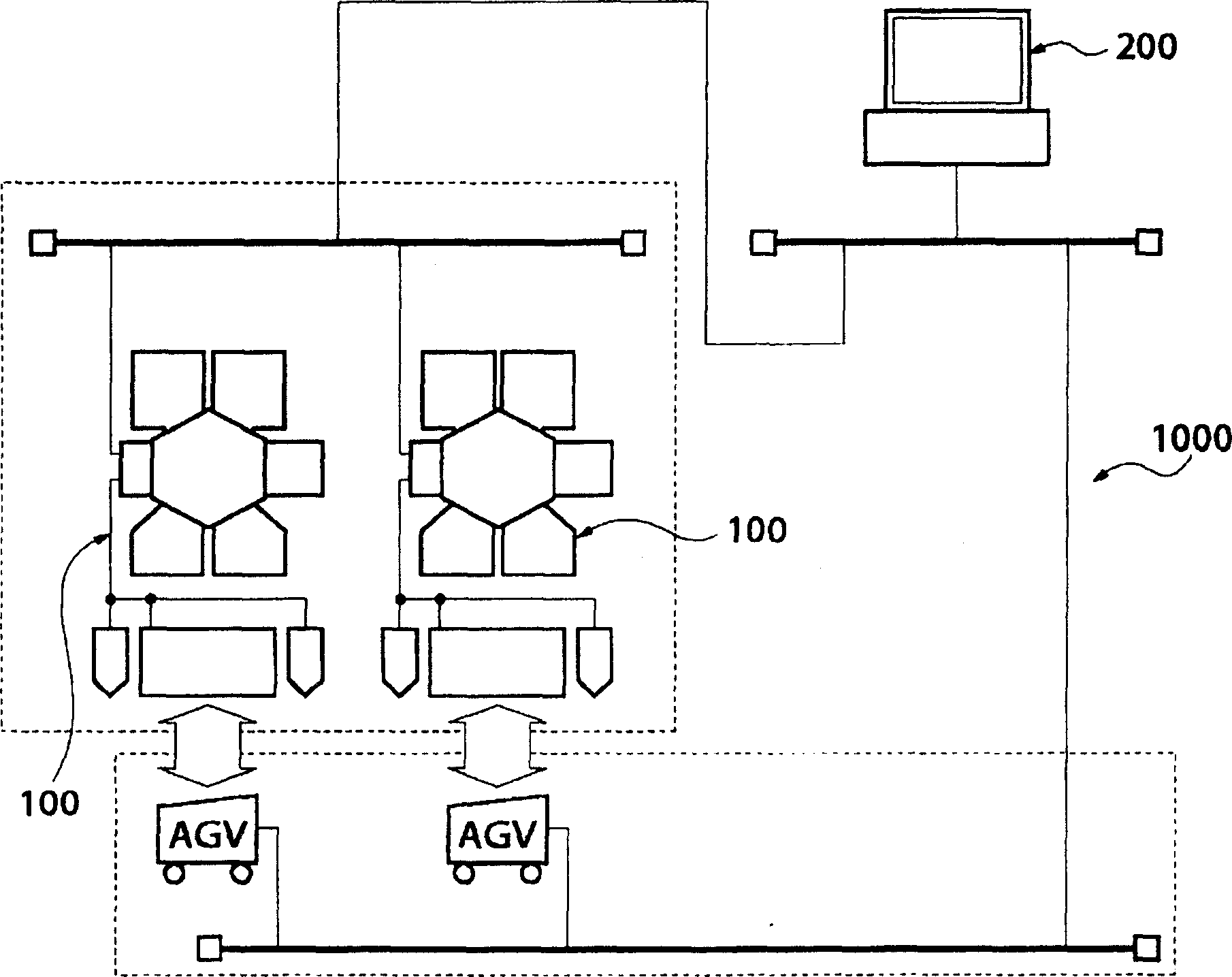
[0079] figure 1 It is a schematic block diagram showing the configuration of a substrate processing system including the substrate processing apparatus of the present embodiment.

[0080] figure 1The substrate processing system 1000 shown is provided with: at least one etching processing apparatus 100 as a substrate processing apparatus, and a device for transporting a wafer cassette described later that stores semiconductor substrates (hereinafter referred to as substrates) to the etching processing apparatus 100. An automatic transfer device (AGV: Auto Guided Vehicle), and a host computer (host computer) 200 connected to the AGV and the etching processing device 100 via a network.

[0081] In the host computer 200, transfer recipes, product processing recipes, and simulation processing recipes described later are pre-registered and installed as programs, and the ...


PUM


Abstract

An etching apparatus 100 as the substrate processing apparatus is provided with a rotary arm 103 for carrying a substrate included in a lot, and process chambers 106 and 107 for carrying out etching to the substrate as product processing. The etching apparatus 100 is controlled by a host computer 200 in which a transportation recipe, a recipe for product processing and a recipe for dummy processing are registered. When a chamber neglecting time being each neglecting time of the process chambers 106 and 107 does not become time out, the host computer 200 discriminates that processing atmosphere in the process chambers used for etching to the lot is stable, omits the execution of the dummy processing, and executes etching to the substrate of the lot.

Description

technical field [0001] The present invention relates to a substrate processing apparatus, a substrate processing method, and a program, and particularly relates to a substrate processing apparatus, a substrate processing method, and a program capable of dummy processing. Background technique [0002] In a plasma process for manufacturing a semiconductor chip, a thin film is etched and a metal is deposited on the etched thin film by CVD (Chemical Vapor Deposition) utilizing the interaction between the plasma and the inner wall of the container. Since a large amount of energy is applied by high frequency or the like in the container, the interaction between the plasma and the inner wall of the container causes the following major problems. [0003] Plasma CVD is a process for forming a thin film on a substrate, but, of course, also deposits a thin film on the inner wall of a container. On the other hand, in the etching process, the film formed on the substrate is reduced by c...

Claims


Application Information

Patent Timeline
IPC IPC(8): G05B15/02G05B19/418H01L21/02
CPCY02P90/02
Inventor 山崎悟史桥本充
Owner TOKYO ELECTRON LTD
Why Eureka
Try Eureka