Wiring structure

A wiring structure and wiring technology, applied in the direction of multilayer circuit manufacturing, printed circuit components, etc., can solve the problems of circuit board damage resonance, severe resonance effect parasitic oscillation of circuit board, circuit structure quality degradation, etc., to increase circuit quality, Overcoming the effects of time design, reducing resonance effects and parasitic oscillations

Active Publication Date: 2005-09-07
VIA TECH INC
View PDF0 Cites 5 Cited by
  • Summary
  • Abstract
  • Description
  • Claims
  • Application Information

AI Technical Summary

Problems solved by technology

[0005] In other words, if the plane of each layer is regarded as the parallel plate effect in the capacitor, it can be clearly found that the smaller the distance between the planes of each layer, the more severe the oscillation of resistance and capacitance (RC), such as grounding The plane 12 and the adjacent power plane 13, etc., cause negative effects such as stray capacitance between the layers, which seriously damages the performance (Performance) and frequency response (Response) of the circuit structure of the printed circuit board.
[0006] like figure 2 As shown, it is an example of the frequency response diagram produced by the currently used printed circuit board, where it can be clearly seen that

Method used


Image

  • Wiring structure
  • Wiring structure
  • Wiring structure

Examples


Example Embodiment

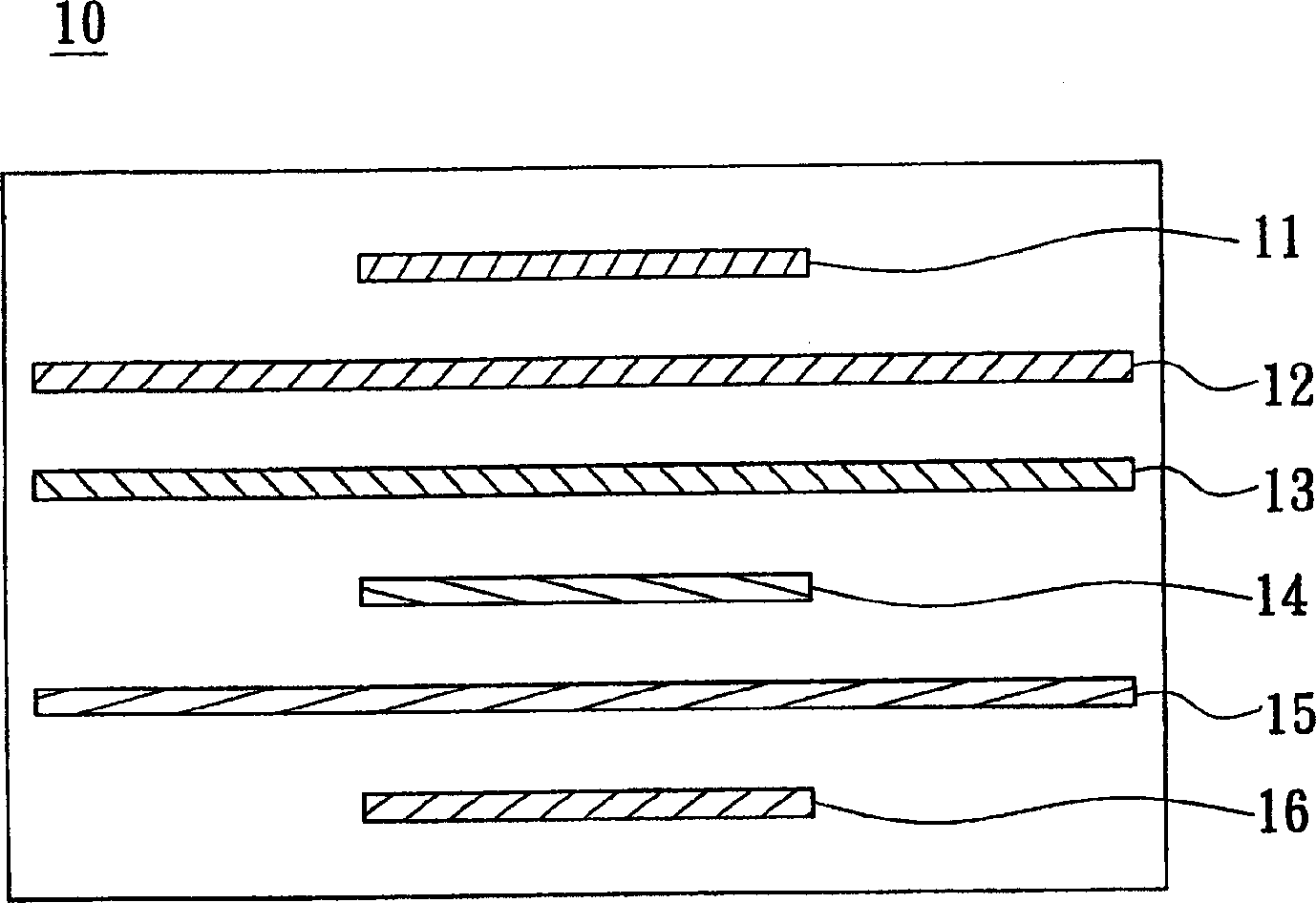
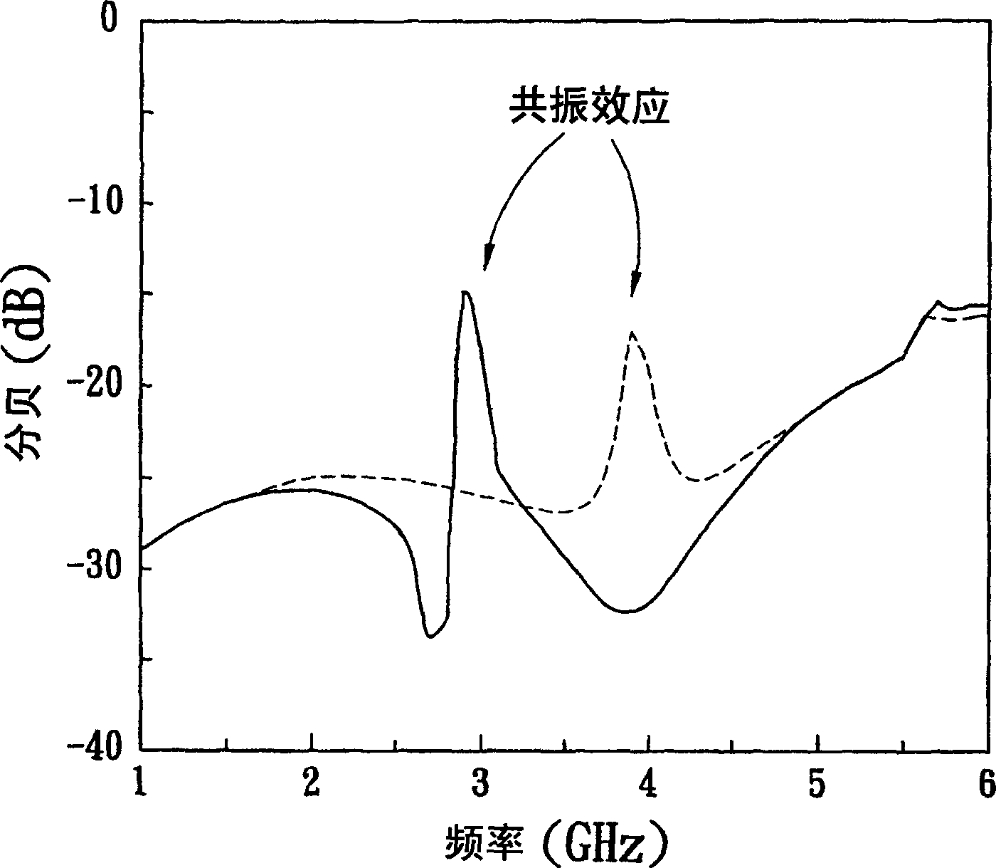
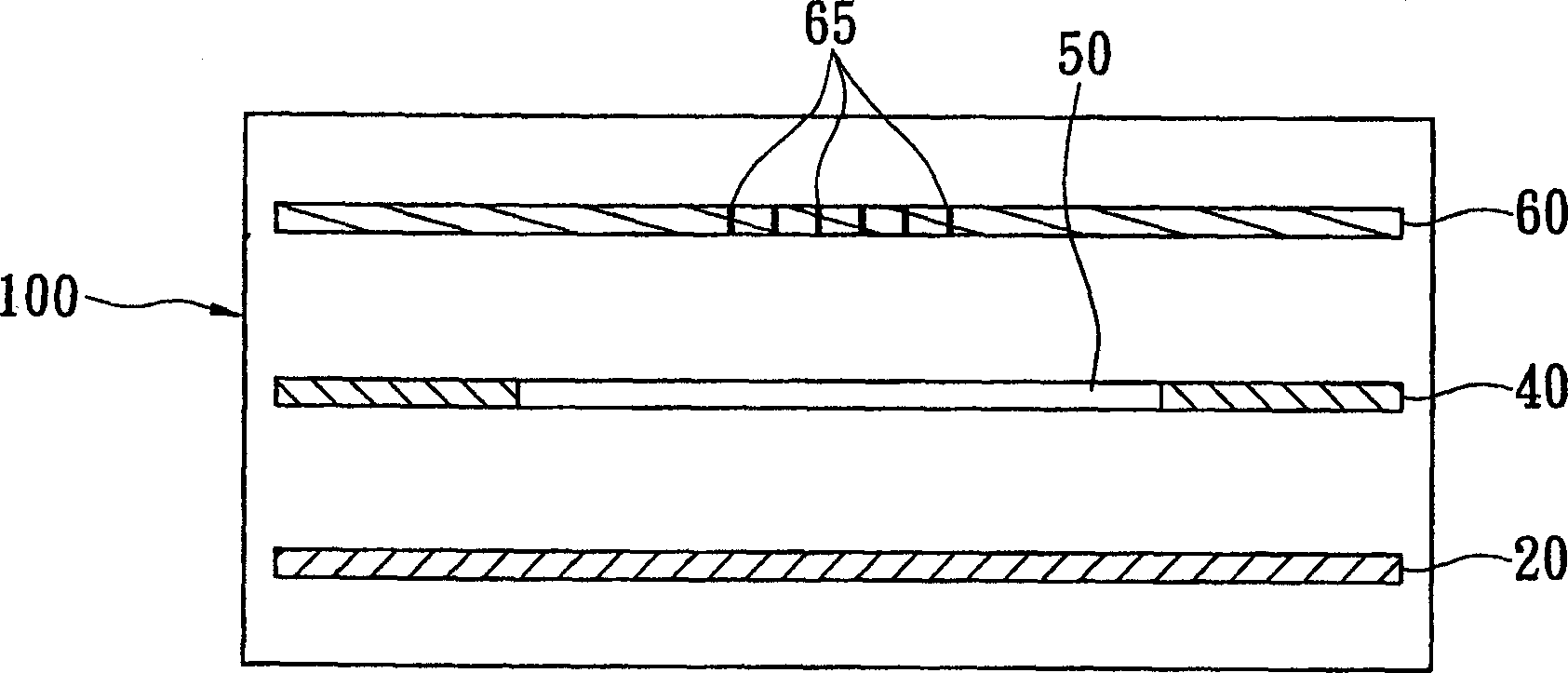
[0027] The main purpose of the present invention is to provide a wiring structure that improves the wiring response, thereby eliminating the poor coupling between the layers of the circuit board and improving the wiring response. First see image 3 A schematic side view of the inner cloth structure of the printed circuit board of the present invention, which shows the inside of the circuit board 100 of a multilayer board, including a ground plane 20, a power plane 40, and a wiring plane 60. However, in practical applications, It may further include various planes (not shown in this figure) such as a component plane, an insulating plane, a dielectric plane, and a signal plane, which are not limited by this embodiment.

[0028] On the wiring plane 60, a plurality of wiring lines 65 are provided to connect the signal transmission between the planes. And a power plane 40 is further provided above or below the wiring plane 60 (in this embodiment, the power plane 40 is located below the...


PUM


Abstract

The invention discloses a wiring structure for improving wiring response, mainly eliminating bad electric coupling between inner-layer planes of a printed circuit board (PCB) to improve the wiring response. The wiring structure makes the wiring able to use a grounding plane as a reference plane and comprises: at least a wiring plane to arrange many signal wires on; and one or many power supply plane, arranged in a PCB and provided with at least an arbitrary shaped etched hole corresponding to the signal wires. And it uses the etching technique to remove the corresponding sections of the power supply planes above or below the signal wires so as to make them able to obtain relatively accurate potentials using the grounding plane as a potential reference, thus reducing the negative influence of stray capacitance between the planes. Further, because of the reduction of the stray capacitance, it can eliminate the resonance effect and parasitic vibration produced as the PCB is at high frequency, so as to improve the circuit quality of the whole PCB.

Description

Technical field [0001] The present invention relates to a technology that enables routing traces to use a ground plane as a potential reference plane, in particular to a wiring structure that improves wiring response, thereby eliminating resonance effects and parasitics generated by circuit boards at high frequencies. Oscillate to improve the overall circuit quality of the circuit board. Background technique [0002] The so-called printed circuit board (print circuit board PCB) refers to a circuit system that can connect electronic components together and make them perform an overall function. The use range of printed circuit boards is very wide, usually in electronic telecommunications, high frequency Circuits, communication systems, aviation, ships, home appliances, automobiles, machinery, instrumentation and other fields must be applied to the related technology of printed circuit boards, and because the technology of integrated circuits (IC) is more and more advanced, the req...

Claims


Application Information

Patent Timeline
IPC IPC(8): H05K1/02H05K3/46
Inventor 李胜源
Owner VIA TECH INC
Why Eureka
Try Eureka