Packaging method for semiconductor image sensing module

A technology of image sensing and packaging method, applied in the direction of semiconductor devices, semiconductor/solid-state device manufacturing, electric solid-state devices, etc., can solve the problems of poor heat dissipation, large size, poor thermal conductivity of plastics, etc. volume effect

Inactive Publication Date: 2005-10-19
邹庆福 +1
View PDF0 Cites 0 Cited by
  • Summary
  • Abstract
  • Description
  • Claims
  • Application Information

AI Technical Summary

Problems solved by technology

[0006] However, in order to connect with external circuits, each metal sheet 82, 84 must still extend a certain distance from the light-transmitting plate 88, such a structure still cannot solve the problem of large volume of the image sensing component after packaging.
[0007] Furthermore, the aforementioned two image sensing components are based on plastic, but the plastic has poor thermal conductivity and is easily deformed, so the entire image sensing component has a problem of poor heat dissipation, so the aforementioned two image sensing components It is still necessary to improve the test components

Method used


Image

  • Packaging method for semiconductor image sensing module
  • Packaging method for semiconductor image sensing module
  • Packaging method for semiconductor image sensing module

Examples


Embodiment Construction

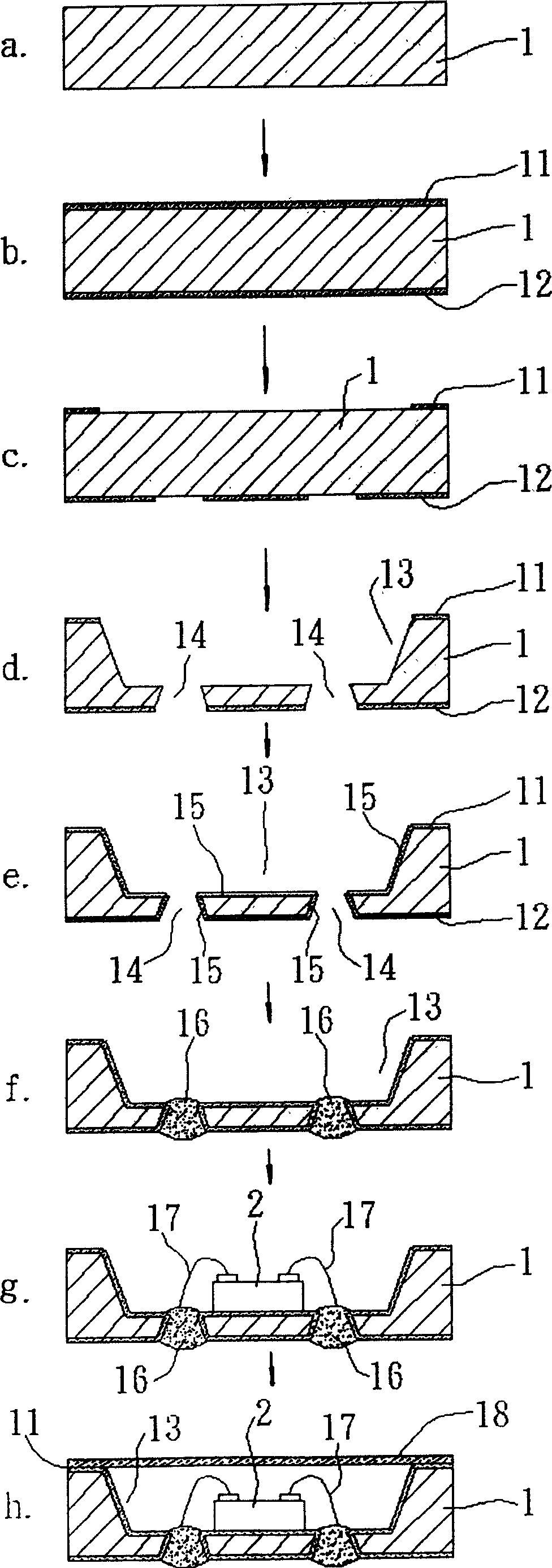
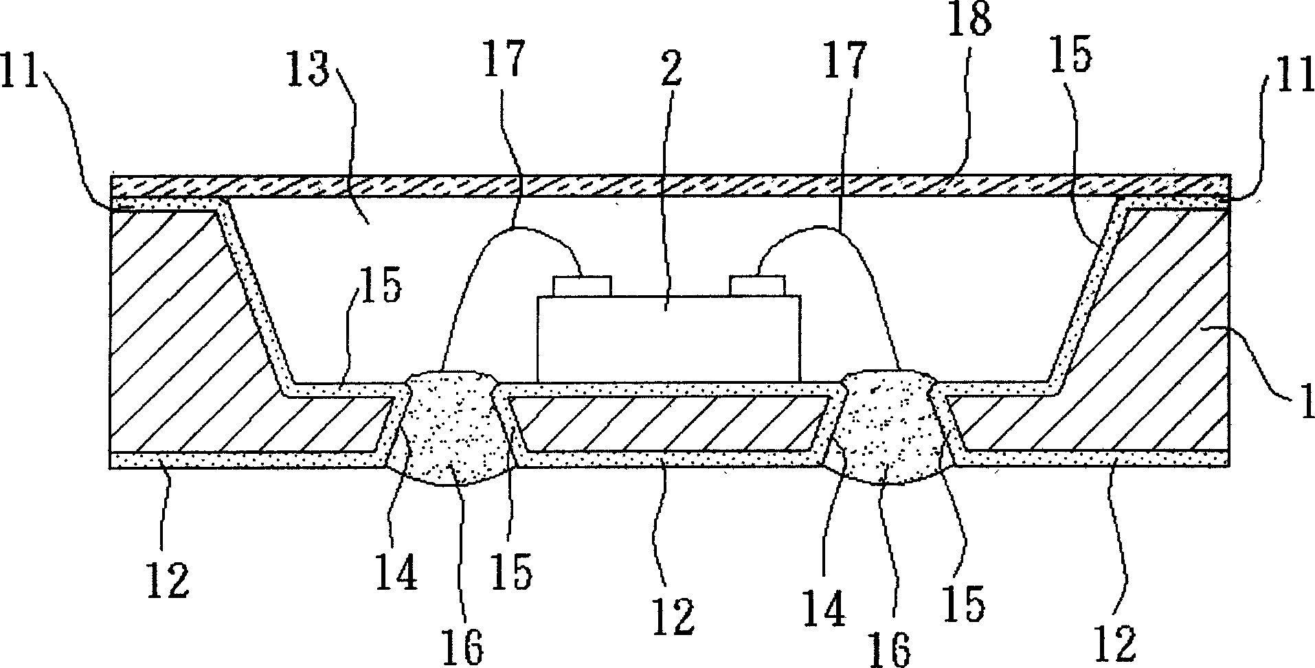
[0046] see figure 1 and FIG. 4, the packaging method of the semiconductor image sensing component of the present embodiment,

[0047] It includes the following steps:

[0048] a. Preparation:

[0049] A single crystal silicon chip is selected as the process substrate 1 .

[0050] b. Form a protective layer:

[0051] The substrate 1 is placed in a furnace tube, and a layer of silicon dioxide is grown on both sides of the substrate 1 by thermal oxidation or a layer of silicon nitride is grown by deposition as a protection layer 11 , 12 .

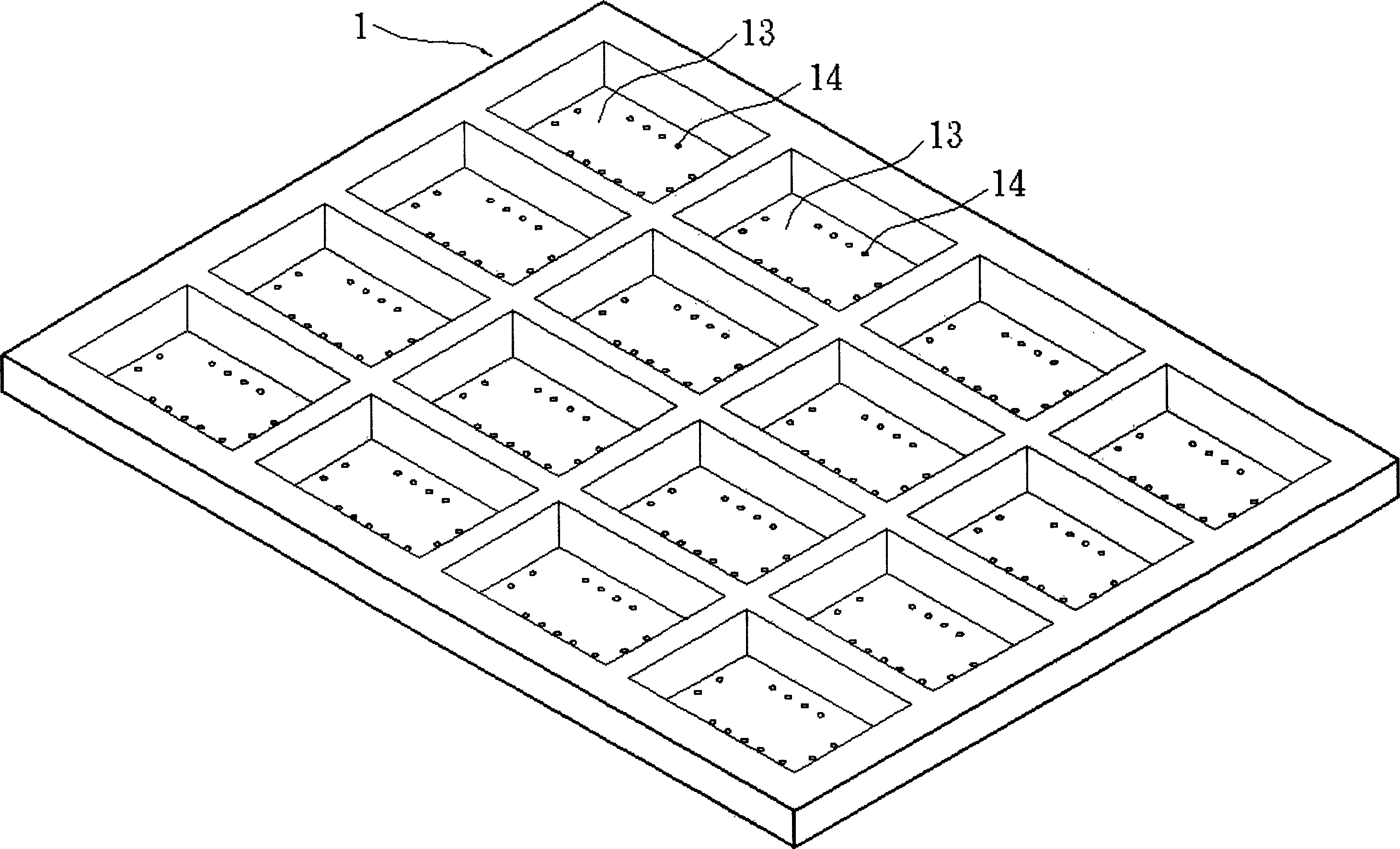
[0052] c. Define the etching hole:

[0053] Part of the protective layer is removed on both sides of the substrate 1 by BOE wet etching or RIE dry etching by lithography process, so that the surface area of ​​the substrate 1 to be etched subsequently is exposed.

[0054] d. Etching:

[0055] Utilize the KOH or TMAH anisotropic wet etching method to etch the parts without the protective layers 11 and 12 on both sides of the substrate 1, ...


PUM


Abstract

A package method for semiconductor image sensing components, which takes monocrystal silicon chips as the process backing to be etched through partly. A containing part is formed on the upper half part of the backing, and several through holes are formed on the lower half part, then an electric insulation layer is formed on the backing surface, then tin balls are heated and pressed to fill and fix the through holes, the image sensing chips are put in the containing part, winding is done among the chip and tin balls of the through holes to finish the electric connection, finally the containing part is sealed by a transparent plate to finish the package.

Description

technical field [0001] The invention relates to a packaging method of a semiconductor image sensing component. Background technique [0002] The structure of the existing image sensor components, such as Taiwan Patent No. 551610 Announcement ( Figure 5 As shown), it is to set several spaced metal sheets 72, 73, 74 on a substrate 71, wherein the metal sheets 72, 74 extend outwards from the substrate 71, and are on the outside of each metal sheet 72, 74 A frame dam 75 is glued to the end, so that a receiving portion 76 is defined between the substrate 71 and the frame dam 75, and an image sensing chip 77 is electrically connected to the metal sheet 73, and the image sensing chip 77 is electrically connected with a wire 78. The chip 77 and the metal sheets 72 and 74 are finally bonded to the frame dam 75 with a light-transmitting plate 79, and the image sensing chip 77 is packaged in the accommodating portion 76 to complete the fabrication of the image sensing component. [0...

Claims


Application Information

Patent Timeline
Patent Type & Authority Applications(China)
IPC IPC(8): H01L21/00H01L21/50H01L27/146
CPCH01L2224/48091H01L2224/97H01L2924/16195
Inventor 邹庆福黄裕盛
Owner 邹庆福
Why Eureka
Try Eureka