

Gallium-indium-nitride-arsenide based epitaxial wafer and hetero-field effect transistor using the same, and its manufacturing method
A technology of field effect transistors and manufacturing methods, which is applied in the direction of semiconductor/solid-state device manufacturing, semiconductor devices, electrical components, etc., and can solve problems such as impracticability
- Summary
- Abstract
- Description
- Claims
- Application Information
AI Technical Summary
Problems solved by technology
Method used
Image

Examples
Embodiment approach 1
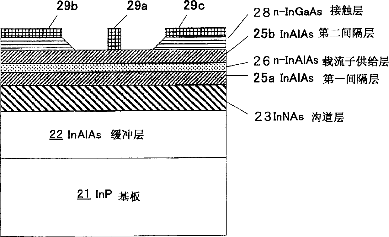
[0061] FIG. 1 is a cross-sectional view showing the structure of a heterogeneous field effect transistor according to Embodiment 1 of the present invention.
[0062] As shown in FIG. 1, the heterogeneous field effect transistor has an InP substrate 21. On the InP substrate 21, an InAlAs buffer layer 22, an InNAs channel layer 23, an InAlAs first spacer layer 25a, an n-InAlAs carrier supply layer 26, and an InAlAs second spacer layer 25b are sequentially stacked. An electrode 29a constituting a gate is formed on the InAlAs second spacer layer 25b, and spaces are provided on both sides of the electrode 29a to form a pair of electrodes 29b and 29c constituting a source electrode and a drain electrode. The electrodes 29b and 29c are formed on the InAlAs second spacer layer 25b through the n-InGaAs contact layer 28.
[0063] Next, we explain the manufacturing method of the heterogeneous field effect transistor constructed in this way.
[0064] In this manufacturing method, a gas source...
Embodiment approach 2
[0066] FIG. 7 is a cross-sectional view showing the structure of a hetero field effect transistor according to Embodiment 2 of the present invention. In FIG. 7, the same reference numerals as those in FIG. 1 indicate the same or equivalent parts.
[0067] As shown in FIG. 7, in the present embodiment, the channel layer is composed of an InNAs layer 23 (a film thickness of 10 nm) as a first channel layer and an InAs layer 24 (a second channel layer) formed on the InNAs layer 23. The film thickness is 4nm) such two types of layer structure. The other points are the same as the first embodiment.
[0068] The reason for this configuration is as explained in Fig. 4 and Fig. 5 at the beginning, because the maximum electron velocity v of the InAs layer d It is larger than the InNAs layer, so in order to make use of the advantages of this InAs layer. When describing in detail, since the InAs channel layer 24 has a lattice mismatch of about 3% with respect to the InP substrate 21, it is im...
Embodiment approach 3
[0074] FIG. 10(a) is a cross-sectional view showing the configuration of a hetero field effect transistor according to Embodiment 3 of the present invention, and FIG. 10(b) is a diagram showing an energy state near the channel layer in FIG. 10(a). In FIG. 10(a), the same reference numerals as those in FIG. 7 indicate the same or equivalent parts.
[0075] As shown in FIG. 10(a), in this embodiment, instead of the InNAs channel layer 23 of Embodiment 2, a GaInNAs channel layer 23 is formed as the first channel layer. The other points are the same as the second embodiment.
[0076] In the second embodiment, since the InNAs layer 23 is used as the first channel layer to facilitate crystal growth, there is a concern that carriers may overflow from the InAs layer 24 as shown in FIG. 8(a). Therefore, in this embodiment, instead of the InNAs channel layer 23, we tried to form a GaInNAs channel layer 23 in which Ga is added to InNAs to increase the band gap.
[0077] In Fig. 6 the same as...
PUM
| Property | Measurement | Unit |
|---|---|---|
| Thickness | aaaaa | aaaaa |
Abstract
Description
Claims
Application Information