Method for implanting ions in semiconductor device

A technology of ion implantation and semiconductor, which is applied in semiconductor/solid-state device manufacturing, instruments, table utensils, etc., and can solve problems such as differences

Active Publication Date: 2005-11-16
SK HYNIX INC
View PDF0 Cites 10 Cited by
  • Summary
  • Abstract
  • Description
  • Claims
  • Application Information

AI Technical Summary

Problems solved by technology

For example, even if the level of uniformity of ion implantation is very high, the semiconductor device par

Method used


Image

  • Method for implanting ions in semiconductor device
  • Method for implanting ions in semiconductor device
  • Method for implanting ions in semiconductor device

Examples


Embodiment Construction

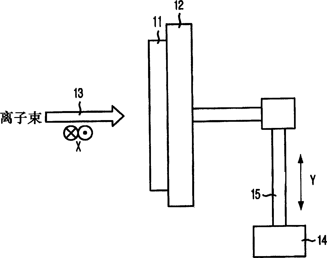
[0033] The ion implantation method in the semiconductor device according to the first embodiment of the present invention will be described in detail with reference to the accompanying drawings.

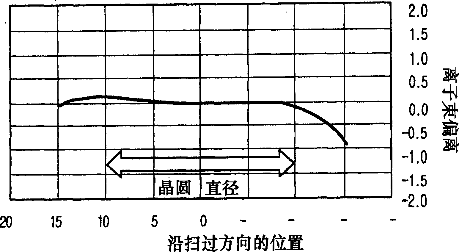
[0034] According to the present invention, the reciprocating scanning speeds in the X and Y directions are set differently according to the position of the substrate used in the non-uniform ion implantation method.

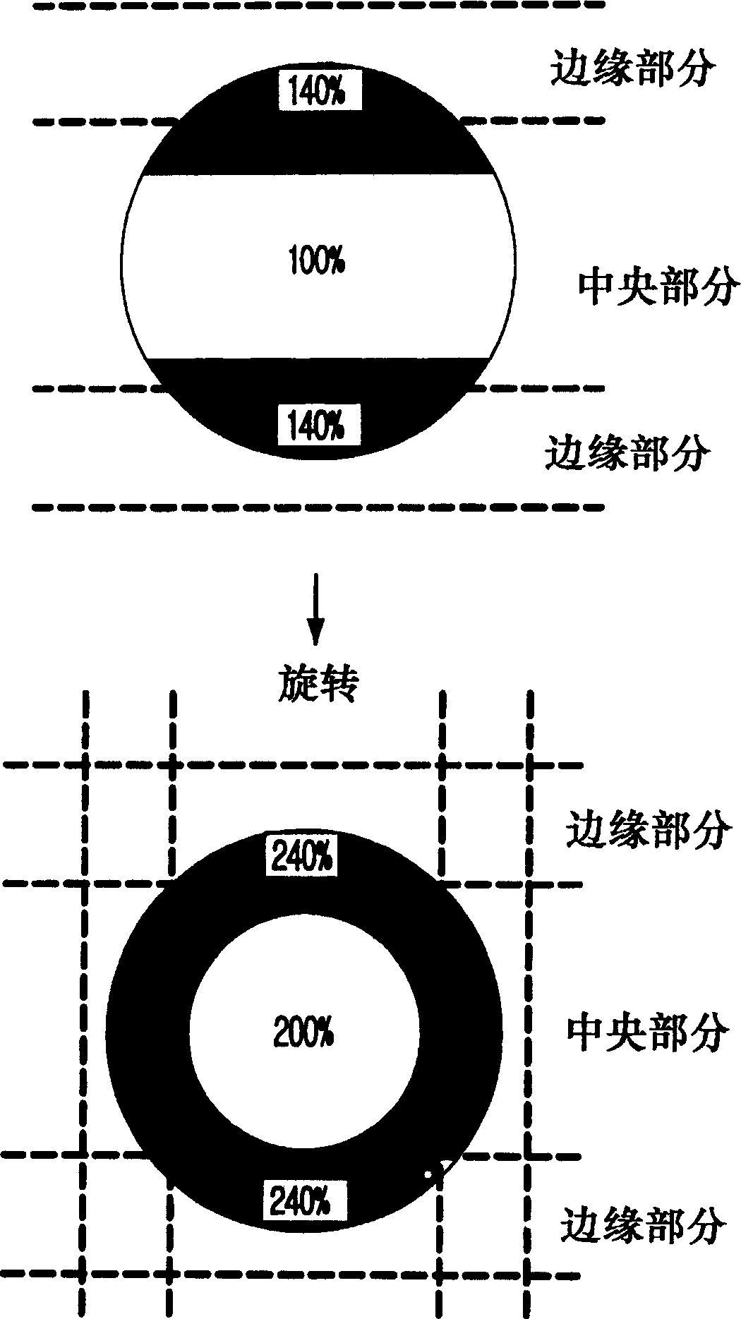
[0035] The present invention is based on a technical principle to identify the critical dimension (CD) of a gate in a substrate without causing differences in semiconductor device parameters in the substrate by performing a non-uniform ion method.

[0036] For example, if the CD of the gate in the central portion of the semiconductor is greater than in the edge portion of the substrate, the central portion of the semiconductor device will have a higher threshold voltage (V T ). Therefore, at the threshold voltage (V T ), for example, by non-uniform ion implantation, th...


PUM


Abstract

PROBLEM TO BE SOLVED: To provide a method for implanting ions into a semiconductor board which method compensates a threshold voltage gap between the central portion and the peripheral portion of the board created, as a result of uniformly implanting ions into the entire surface of the board, and to provide a manufacturing method for a semiconductor element which the manufacturing method improves the nonuniformity of transistor characteristics in the board.

Description

technical field [0001] The present invention relates to a method for manufacturing a semiconductor device, and more particularly to a method for implanting ions into a semiconductor device. Background technique [0002] Recently, more precise control of impurities is in line with the trend in volume and density of large semiconductor devices. In addition, remanufacturing and processing capabilities are required in view of mass-manufacturing techniques. Therefore, the practical application of the ion implantation method becomes more important. This ion implantation method ionizes the impurity and accelerates it by scanning the impurity in a predetermined area on a substrate, thereby implanting a predetermined amount of the impurity in the desired area. [0003] The ion implantation method described above can selectively implant impurities and implant impurities with high purity. Furthermore, this ion implantation method can control impurities more precisely, thereby provid...

Claims


Application Information

Patent Timeline
IPC IPC(8): H01L21/265
CPCA47G21/14G09F23/08
Inventor 孙容宣秦丞佑李民镛卢径奉
Owner SK HYNIX INC
Why Eureka
Try Eureka