

Dry etch post process method
A technology of dry etching and processing chambers, which is applied in the field of semiconductor manufacturing technology, can solve the problems of product electrical connection errors, low yield, and difficulty in completely removing polymers, etc., to achieve the effect of improving product yield and avoiding electrical connection errors
- Summary
- Abstract
- Description
- Claims
- Application Information
AI Technical Summary
Problems solved by technology
Method used
Image

Examples
Embodiment Construction
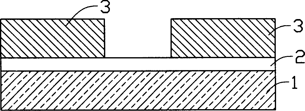
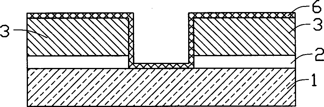
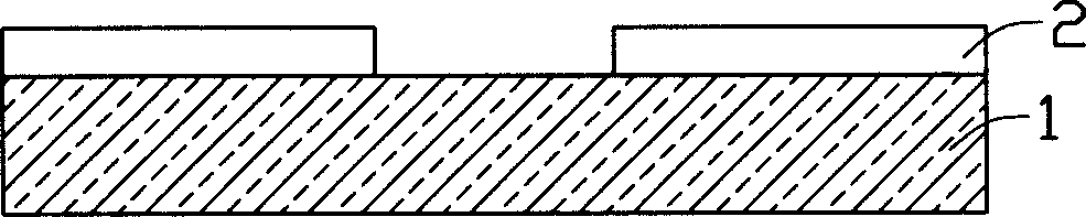
[0014] see Figure 4 to Figure 8 , is a schematic diagram of dry etching to form the source and drain layers (Sourceelectrode&Drain electrode, SD) of the thin film transistor. see Figure 4 , is a deposition step, depositing the SD metal layer 50 on the glass substrate 10 , and then depositing a passivation layer 40 on the SD metal layer 50 and the substrate 10 . see Figure 5 , is a photomask process, coating photoresist on the passivation layer 40, and then exposing the photoresist through a photomask to form the photoresist layer 30 with openings. see Figure 6 , is a dry etching step, using O in a dry etching chamber (not shown) 2 , SF 6 and CF 4 The gas etches a portion of the passivation layer 40 to form a contact hole 70, during which a polymer layer 60 is formed and covers the contact hole 70 and the like. see Figure 7 , is a post-dry etch processing step using SF 6 Ashing is performed to remove the polymer layer 60 . see Figure 8 , is a photoresist stripp...
PUM
 Abstract
Description
Claims
Application Information