Method of forming capacitor of semiconductor device

A technology for semiconductors and capacitors, applied in the field of capacitors, which can solve the problems of low crystallization temperature, increased leakage current, difficult to use as leakage current characteristics and charging capacitor dielectric film, etc.

Inactive Publication Date: 2006-01-18
SK HYNIX INC
View PDF0 Cites 5 Cited by
  • Summary
  • Abstract
  • Description
  • Claims
  • Application Information

AI Technical Summary

Problems solved by technology

[0009] However, since the crystallization temperature is higher than that of Al 2 o 3 The crystallization temperature is lower, if a high-temperature thermal process of 750°C or higher is performed when the upper electrode is formed of doped polysilicon, or 600°C or higher is implemented when the upper electrode is formed of a metallic material (such as TiN) High temperature thermal process, there are still problems: HfO 2 The dielectric film is crystallized and impurities are diffused from the upper electrode into the dielectric film, so the leakage current increases
[0010] Therefore, currently Al 2 o 3 membrane and HfO 2 It is difficult for the film to be a dielectric film that can ensure the required leakage current characteristics and charging capacitance.

Method used


Image

  • Method of forming capacitor of semiconductor device
  • Method of forming capacitor of semiconductor device
  • Method of forming capacitor of semiconductor device

Examples


Embodiment Construction

[0019] Hereinafter, preferred embodiments of the present invention will be described with reference to the drawings.

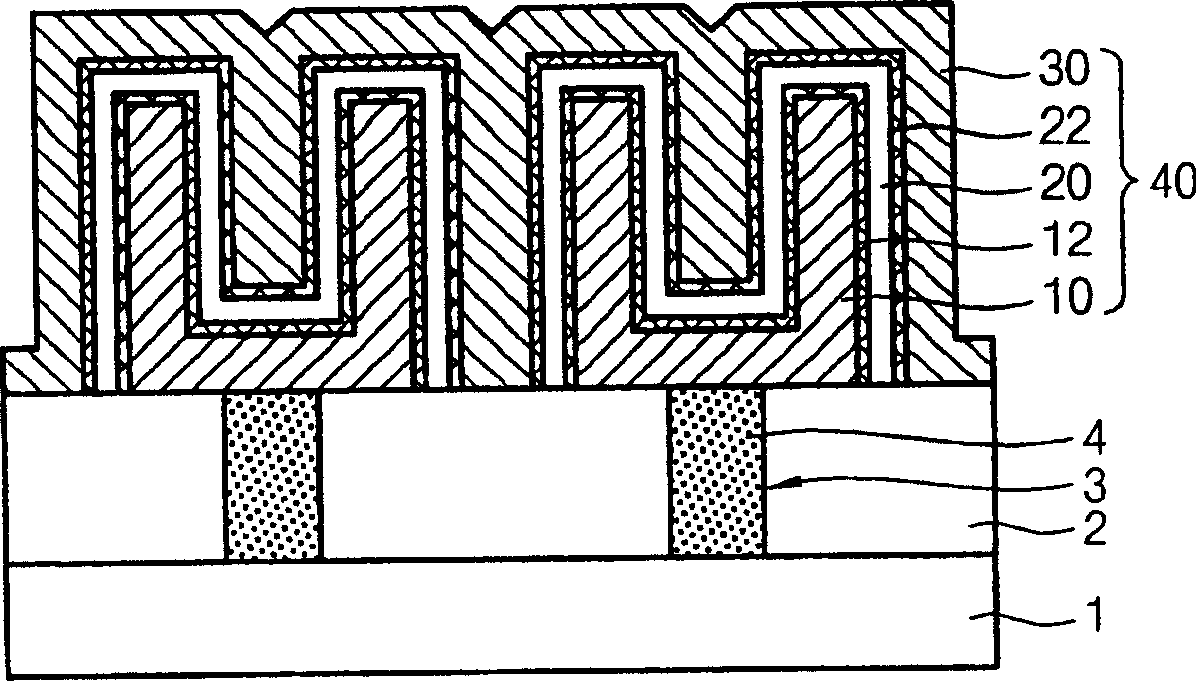
[0020] Involving the technical principle of the present invention, the present invention utilizes nitrided La 2 o 3 The dielectric film forms a capacitor as a dielectric film, thereby overcoming the Al 2 o 3 Dielectric properties of films and HfO 2 The limitation of the thermal stability of the film. In addition, in the formation of nitrided La 2 o 3 film process, the La 2 o 3 After film deposition, by means of NH 3 La 2 o 3 The low-temperature plasma nitridation performed on the surface of the film introduces nitrogen into La 2 o 3 film, La-O-N bonds are formed.

[0021] In this case, since La 2 o 3 Nitriding of the surface of the film, La 2 o 3 The crystallization temperature of the film itself is increased, and impurities are also prevented from diffusing from the lower electrode and the upper electrode to the La 2 o 3 inside the membrane...


PUM


Abstract

Disclosed is a method of forming a capacitor of a semiconductor device which can secure a desired leakage current characteristic while securing a desired charging capacitance. The inventive method of forming a capacitor of a semiconductor device comprises steps of: forming a bottom electrode on a semiconductor substrate with a storage node contact so that the bottom electrode is connected with the storage node contact; plasma-nitrifying the bottom electrode to form a first nitrification film on the surface of the bottom electrode; forming a La2O3 dielectric film on the bottom electrode including the first nitrification film; plasma-nitrifying the La2O3 dielectric film to form a second nitrification film on the surface of the La2O3 dielectric film; and forming a top electrode on the La2O3 dielectric film including the second nitrification film.

Description

technical field [0001] The present invention relates to a method of forming a capacitor of a semiconductor device; more particularly, to a method of forming a capacitor of a semiconductor device capable of ensuring leakage current characteristics and required charging capacitance at the same time. Background technique [0002] Recently, as the development of semiconductor manufacturing technology accelerates the high integration of storage products, the unit cell area is greatly reduced, and the operating voltage is also reduced. However, despite the reduced cell area, the charging capacitance required to operate the memory device must still be high enough, not less than 25fF per cell, to prevent read errors from occurring and refresh time to be reduced. [0003] Therefore, even if a three-dimensional storage electrode having a hemispherical electrode surface is used for a nitrogen oxide (NO) capacitor of a dynamic random access memory (DRAM), the capacitor uses Si deposited...

Claims


Application Information

Patent Timeline
Patent Type & Authority Applications(China)
IPC IPC(8): H01L21/329H01L21/82H01L21/8239H01L21/8242H01L21/02H01L21/314H01L21/316H01L21/321H01L21/8244H01L27/108
CPCH01L28/56H01L27/10852H01L28/65H01L21/3143H01L27/10817H01L28/90H01L21/31604H01L21/3211H01L21/31616H01L21/02192H01L21/02205H01L21/0217H01L21/02178H01L21/02252H01L21/02247H01L21/022H01L21/02271H01L21/0228H10B12/318H10B12/033H01L21/31H10B99/00H10B12/00H01L21/0234
Inventor 李起正
Owner SK HYNIX INC
Why Eureka
Try Eureka