Image pickup device and camera module

A technology of image pickup device and wiring diagram, which is applied in the direction of camera, camera body, image communication, etc., and can solve problems such as bad signal, signal becoming noise, and image quality degradation

Inactive Publication Date: 2006-01-18
SHARP KK
View PDF1 Cites 5 Cited by
  • Summary
  • Abstract
  • Description
  • Claims
  • Application Information

AI Technical Summary

Problems solved by technology

[0013] In the case where the conventional camera module 10 configured as described above is applied to a mobile phone having a camera, when the camera module 10 receives electric signals from the main body of the mobile phone other than the camera part and electric devices other than the mobile phone , problems can arise such as reduced image quality of captured images and / or malfunction of the camera itself
[0017] (1) Electrical signals from inside the mobile phone and from outside the mobile phone pass through the camera module 10 and are added as noise to the electrical signal of the image pickup device 6, and thus the image quality of the captured image is degraded
In particular, in the case of a mobile phone, when a signal from a high frequency (RF) unit passes through the camera module 10, the image quality tends to degrade easily.
The reason for this is that mobile phones operate at a high frequency and have a large output power
[0018] (2) The signal generated in the image pickup device 6 becomes noise and exerts a bad influence on the signal of the mobile phone body other than the camera module 10
[0019] (3) A signal generated in the image pickup device 6 becomes noise and causes malfunction of electric devices existing outside the mobile phone
[0020] The problem (1) is generated when the camera module 10 receives noise from the body part of the mobile phone other than the camera module 10 and noise from electrical devices other than the mobile phone
Problems (2) and (3) arise when noise from the camera module 10 causes malfunctions in other electronic devices
[0021] In order to prevent these problems, Patent Document 1 proposes to protect the camera module from electromagnetic radiation by making the camera case conductive; but according to this shielding method, only the camera case of the camera module is shielded, and the optical opening unit such as the lens unit is shielded. is not blocked
Therefore, the captured image may be badly affected by the noise going in and out through the lens unit

Method used


Image

  • Image pickup device and camera module
  • Image pickup device and camera module
  • Image pickup device and camera module

Examples


no. 1 approach

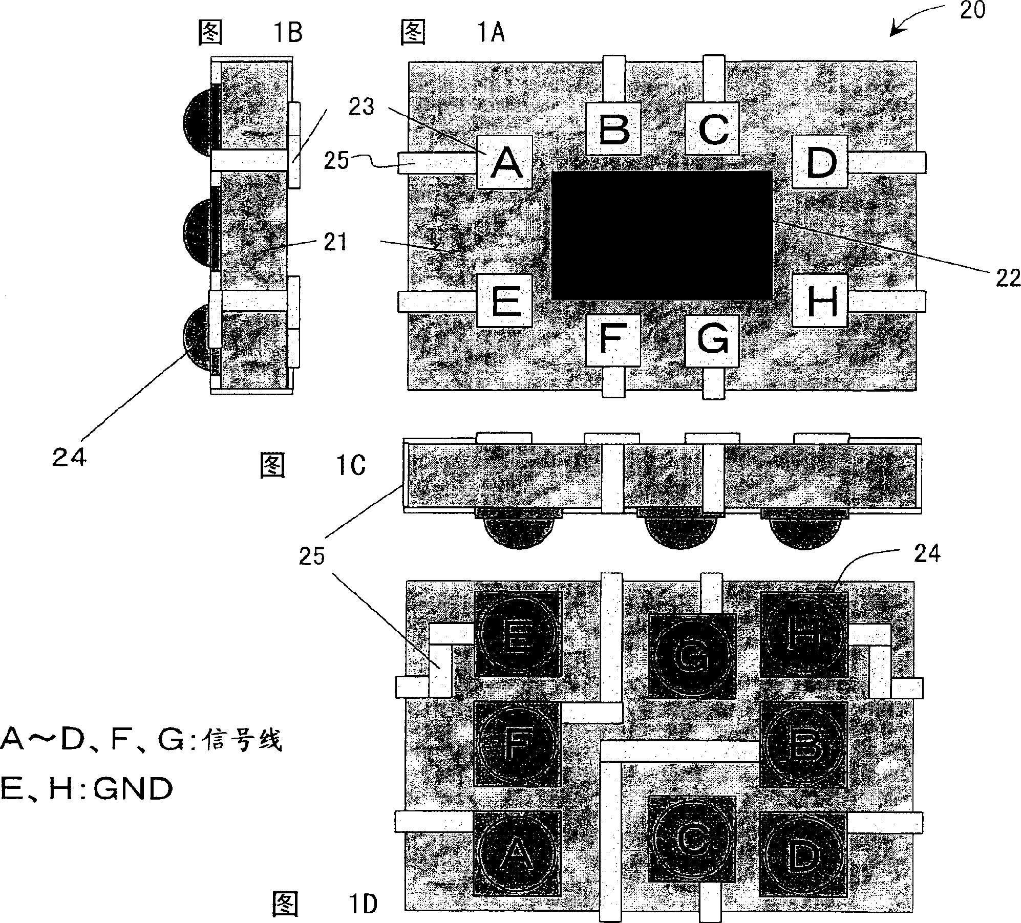
[0069] 1A is a plan view showing an example structure of an image pickup device according to a first embodiment of the present invention. FIG. 1B is a side view viewed from the left side of FIG. 1A . Fig. 1C is a side view as viewed from the bottom side of Fig. 1A. FIG. 1D is a bottom view of FIG. 1A.

[0070] As shown in FIGS. 1A to 1D , the image pickup device 20 is constituted by a CCD image sensor or a CMOS image sensor or the like that converts incident light from the outside (light from an object) into an electric signal. A light receiving unit 22 for light from an object is provided in a central portion of the surface of an image pickup device main body unit (device main body unit) 21 . The light receiving unit 22 is included in an image pickup unit that forms an image of an object by converting incident light into an electrical signal (optical signal). Electrodes 23 (bonding sheets) are provided around the light receiving unit 22 . Protruding electrodes 24 (solderi...

no. 2 approach

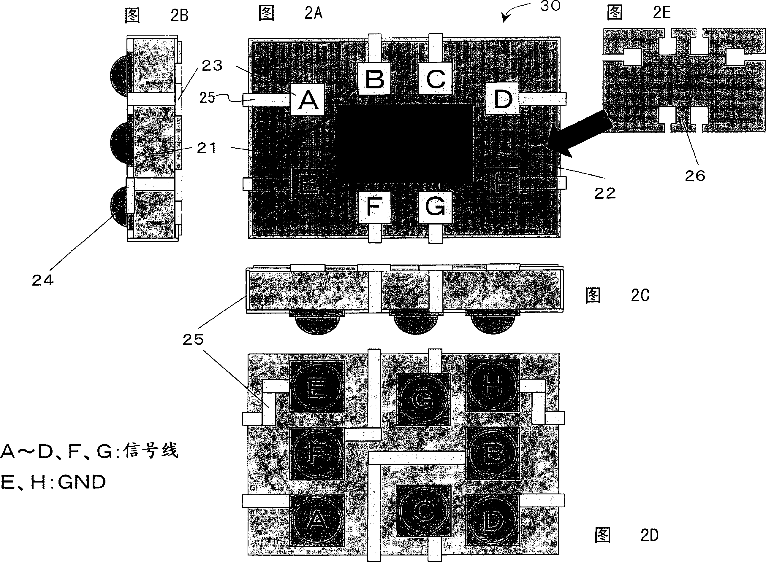
[0090] In the first embodiment, the light-transmitting conductive layer 26 is provided in the signal wiring portion (the electrode 23 : A to D, F and G and the wiring pattern 25 connected thereto and the portion of the conductive unit of the power supply wiring portion has one or more openings in it. However, in the second embodiment, the surface of the image pickup device main body unit 21 is covered with the light-transmitting insulating layer 27 which will be described later at the portion corresponding to the ground wiring (electrodes 23: E and H and There are one or more openings in the portion of the conductive unit connected thereto to the wiring pattern 25 ), and furthermore, a light-transmitting conductive layer 26A to be described later is provided over the light-transmitting insulating layer 27 .

[0091] 5A is a plan view of a second embodiment of the image pickup device of the present invention. Fig. 5B is a side view viewed from the left side of Fig. 5A. Fig. 5...

no. 3 approach

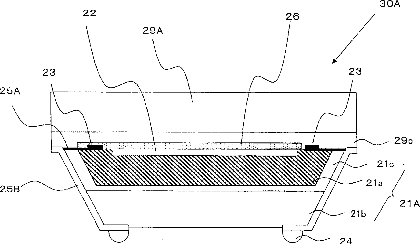
[0110] In the first and second embodiments, the front side of the image pickup device main body unit 21 (or 21A) is covered with the light-transmitting conductive layer 26 or 26A, and thus its inside is magnetically shielded. In the third embodiment, similarly to the case of having the light-transmitting conductive layer 26 or 26A, the back side (which may also include side surfaces) is also additionally covered with the light-transmitting conductive layer.

[0111] In the case of the back surface of the image pickup device main body unit 21, similarly to the case where the light-transmitting conductive layer 26 is provided on the front surface, the light-transmissive conductive layer is formed in a position corresponding to the protrusion provided on the back surface side of the image pickup device main body unit 21. The electrode 24 (soldering bump) and the wiring pattern 25 connected thereto, the signal wiring portion (bump electrodes 24; A to D, F and G and the wiring patte...


PUM


Abstract

The surface of the image pickup device 21 is covered by a transparent conductive member 26 that is made of, for example, a transparent conductive past resin and that is electrically connected to a ground potential GND. By having this arrangement, it is possible to electromagnetically shield the image pickup device 30 itself. The transparent conductive member 26 has one or more openings in the parts that correspond to the conductive unit of the signal wiring portion (the electrodes 23; A to D, F, and G, and the wiring patterns 25 that are connected thereto), out of the electrodes 23 and the wiring patterns 25 provided on the front surface side of the image pickup device body unit 21.

Description

technical field [0001] The present invention relates to an image pickup device such as a CMOS image sensor and a CCD image sensor used as an image pickup unit in a video camera, a digital still camera, a mobile phone with a camera, a portable information terminal device with a camera, etc., It also relates to a camera module comprising such an image pickup device. Background technique [0002] A conventional camera module of this type will be described below with reference to the accompanying drawings. [0003] 9A is a sectional view of main parts showing an example structure of a conventional camera module. Figure 9B is a bottom view of the camera module shown in FIG. 9A. Figure 9A is Figure 9B Sectional view of the line A-A' in. [0004] Figure 9A and Figure 9B As shown, a camera module 10 includes a lens cap 1, a lens 2, a lens barrel 3 for accommodating the lens 2, an IR (infrared ray) cut filter 4, a camera case 5 for accommodating these components, an image pickup...

Claims


Application Information

Patent Timeline
Patent Type & Authority Applications(China)
IPC IPC(8): H04N5/335H04N5/225H01L27/14G03B17/02H01L27/146H01L31/0216H01L31/0232H04N5/357H04N101/00H05K9/00
CPCH01L27/14618H04N5/2257H01L2224/13H01L2224/48091H01L2224/48227H04N23/57H01L2924/00014H01L27/146H04N25/00H04N25/60
Inventor 谷田好范福田宏昭东条行雄
Owner SHARP KK
Why Eureka
Try Eureka