Preparation method of electroluminescent device containing silicon based rear-earth-doped luminous material

A technology of electroluminescent devices and luminescent materials, which is applied in the direction of luminescent materials, electroluminescent light sources, chemical instruments and methods, etc., and can solve the problems such as the effective doping concentration cannot be too high, the concentration is quenched, and the luminescent characteristics are reduced.

Inactive Publication Date: 2006-01-25
INST OF SEMICONDUCTORS - CHINESE ACAD OF SCI
View PDF0 Cites 11 Cited by
  • Summary
  • Abstract
  • Description
  • Claims
  • Application Information

AI Technical Summary

Problems solved by technology

[0005] However, the doping of silicon-based rare earth materials also has its limitations, that is, its effective doping concentration cannot be too high, and high doping conce

Method used


Image

  • Preparation method of electroluminescent device containing silicon based rear-earth-doped luminous material
  • Preparation method of electroluminescent device containing silicon based rear-earth-doped luminous material
  • Preparation method of electroluminescent device containing silicon based rear-earth-doped luminous material

Examples


Embodiment Construction

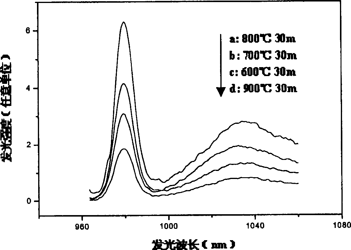
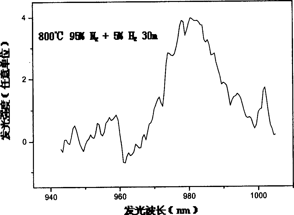
[0038] On the basis of our many experiments, the present invention proposes a silicon-based rare earth-doped luminescent material that is fully compatible with the existing microelectronic technology and can realize high-efficiency room-temperature luminescence and an electroluminescent device containing the material. Studies have shown that the addition of an appropriate proportion of impurity elements can significantly increase the effective doping degree of rare earth materials in silicon-based silicon dioxide films, and realize the room temperature efficient luminescence of rare earth-doped silicon-based silicon dioxide film materials; Compared with impurity elements, the luminous intensity and temperature quenching effect are significantly improved.

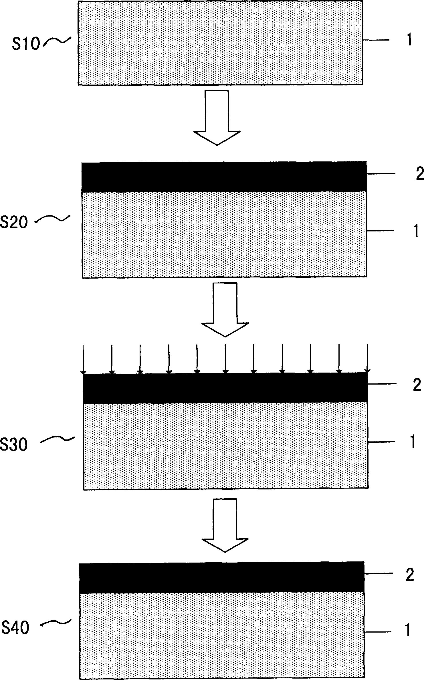
[0039] see Figure 6 As shown, the present invention contains a silicon-based rare earth-doped luminescent material electroluminescent device, on the basis of rare earth ion implantation, a large amount of impurity ion impla...


PUM


Abstract

An electro-fluorescence component containing luminous material with silicon based rare-earth-doped consists of a p - type or n - type silicon substrate , a doping layer formed by injecting ion silica grown on silicon substrate and used as active region of luminous component , a n - type or p - type poly-silicon layer formed on doping layer , a silica isolation layer grown on doping and poly-silicon layer , an electrode on n - type or p - type poly-silicon layer , another electrode on p - type or n - type silicon substrate and an opening for light outgoing on silica isolation layer surface .

Description

technical field [0001] The invention relates to an electroluminescence device and a preparation method, in particular to a preparation method of an electroluminescence device containing a silicon-based rare earth doped luminescent material. Background technique [0002] With the development of VLSI technology, the integration of chips is getting higher and higher. All aspects of people's life, production and national defense require faster and faster integrated circuit chip computing speed. However, due to the sharp reduction of the line width of the integrated circuit process in the past 20 years, the operation speed of a single MOS transistor is getting faster and faster, and the operation speed of the integrated circuit chip by improving the operation speed of a single transistor is due to physical effects. Reaching the limit; and with the improvement of chip integration, it is often not the operation speed of a single transistor that restricts the operation speed of the...

Claims


Application Information

Patent Timeline
IPC IPC(8): H05B33/20H05B33/14H05B33/12H05B33/10C09K11/00
Inventor 张建国成步文余金中王启明
Owner INST OF SEMICONDUCTORS - CHINESE ACAD OF SCI
Why Eureka
Try Eureka