Reflective electrode and compound semiconductor light emitting device including the same

一种反射电极、发光器件的技术,应用在半导体器件、半导体激光器、半导体/固态器件制造等方向,能够解决FCLED特性不稳定、FCLED短寿命等问题,达到优良欧姆接触特性、低工作电压、低光吸收系数的效果

Inactive Publication Date: 2006-04-12
SAMSUNG ELECTRONICS CO LTD
View PDF1 Cites 4 Cited by
  • Summary
  • Abstract
  • Description
  • Claims
  • Application Information

AI Technical Summary

Problems solved by technology

Therefore, there are disadvantages in that the FCLED to which the reflective electrode is applied has a short lifespan, and the characteristics of the FCLED are unstable.

Method used


Image

  • Reflective electrode and compound semiconductor light emitting device including the same
  • Reflective electrode and compound semiconductor light emitting device including the same
  • Reflective electrode and compound semiconductor light emitting device including the same

Examples


Embodiment Construction

[0023] The present invention will now be described more fully with reference to the accompanying drawings, in which embodiments of the invention are shown.

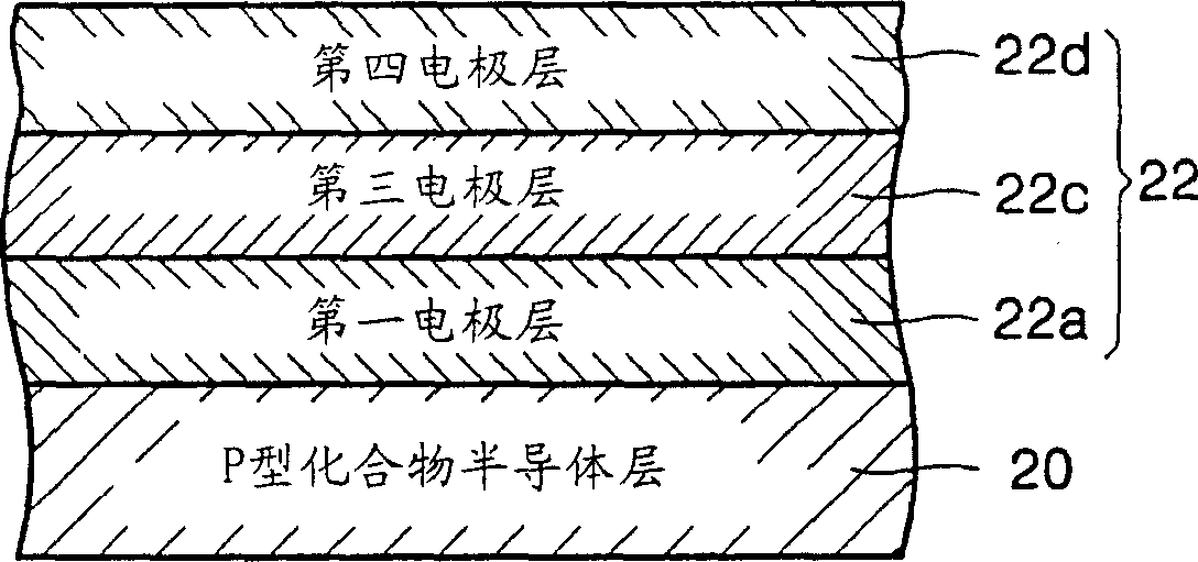
[0024] figure 1 is a sectional view showing a reflective electrode according to a first embodiment of the present invention.

[0025] refer to figure 1 , the reflective electrode 22 is formed on the p-type compound semiconductor layer 20 . The reflective electrode 22 according to the first embodiment of the present invention includes a first electrode layer 22 a , a third electrode layer 22 c and a fourth electrode layer 22 d sequentially formed on the p-type compound semiconductor layer 20 .

[0026] The first electrode layer 22a is in ohmic contact with the p-type compound semiconductor layer 20 . The first electrode layer 22a is formed of one of Ag and Ag alloy with a thickness of 0.1-500 nm. Here, the Ag alloy includes a group consisting of Mg, Zn, Sc, Hf, Zr, Te, Se, Ta, W, Nb, Cu, Si, Ni, Co, Mo, Cr, Mn, Hg, Pr ...


PUM


Abstract

Provided are a reflective electrode and a compound semiconductor light emitting device having the reflective electrode, such as LED or LD is provided. The reflective electrode formed on a p-type compound semiconductor layer of a compound semiconductor light emitting device, comprising a first electrode layer formed one of a Ag and Ag-alloy and forms an ohmic contact with the p-type compound semiconductor layer, a third electrode layer formed of a material selected from the group consisting of Ni, Ni-alloy, Zn, Zn-alloy, Cu, Cu-alloy, Ru, Ir, and Rh on the first electrode layer, and a fourth electrode layer formed of a light reflective material on the third electrode layer.

Description

technical field [0001] The present invention relates to a reflective electrode and a compound semiconductor light emitting device including the same, and more particularly, to a reflective electrode having low contact resistance, high reflectance and improved electrical conductivity and a compound semiconductor light emitting device having the same device. Background technique [0002] Compound semiconductor light-emitting devices can convert electrical signals into light using the properties of compound semiconductors. Recently, laser light of a semiconductor laser diode such as a light emitting diode (LED) or a laser diode (LD) is actually used in the field of application, such as in optical communication, multiplex communication, or space communication. Semiconductor lasers are widely used as light sources for transmitting data, recording data, or reading data in devices such as compact disc players (CDP) or digital versatile disc players (DVDP), or in optical communicat...

Claims


Application Information

Patent Timeline
Patent Type & Authority Applications(China)
IPC IPC(8): H01L33/00H01S5/00H01L33/32H01L33/40
CPCH01S5/0425H01S5/34333H01L33/32H01S5/18H01S5/2027H01L33/405H01L21/28575H01S5/1078B82Y20/00H01S5/04253H01S5/04257
Inventor 金美良郭准燮
Owner SAMSUNG ELECTRONICS CO LTD
Why Eureka
Try Eureka