Structure of dynamic RAM
A dynamic random access and memory technology, applied in static memory, digital memory information, information storage, etc., can solve problems affecting component quality and yield, improve product yield and reliability, and avoid contact short circuit effects
- Summary
- Abstract
- Description
- Claims
- Application Information
AI Technical Summary
Problems solved by technology
Method used
Image
Examples
Embodiment 1
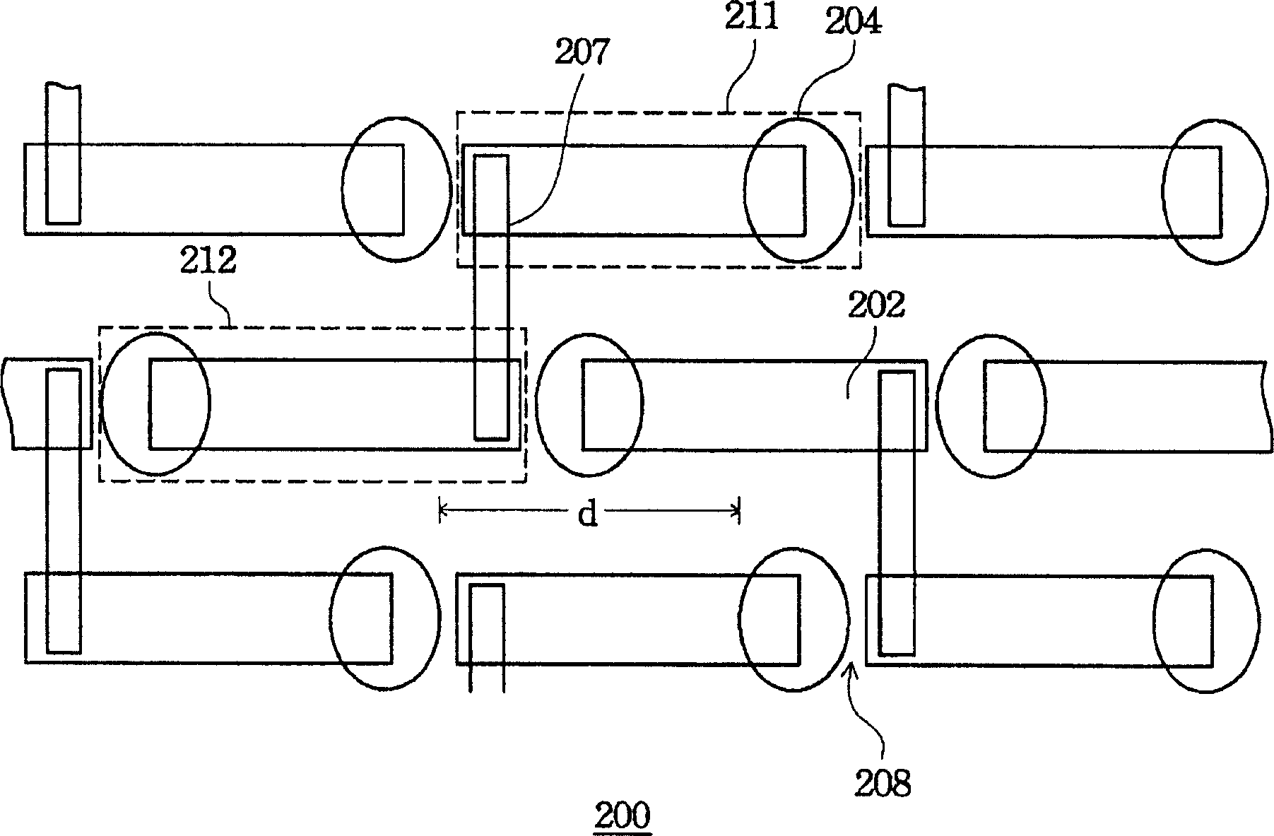
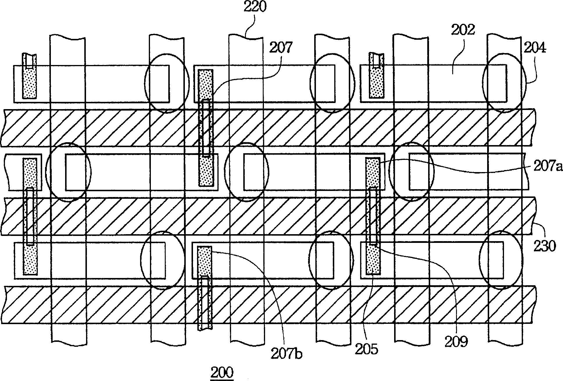
[0047] The present invention discloses a structure of a dynamic random access memory, referring to Figure 2A as shown, Figure 2A What is shown is a partial plan view of the substrate surface of a DRAM device according to the first preferred embodiment of the present invention.
[0048] First of all, the present invention separates the active areas of the mirror-connected design of existing memory cells and forms dislocations, as Figure 2A As shown in , the substrate 200 has independent active regions 202, and the deep trench patterns 204 are arranged in a checkerboard manner on each active region 202, wherein the active region 202 is, for example, a P-type silicon base The material is used as the lower electrode, and the inside of the deep trench pattern 204 is a capacitor structure. At the same time, the present invention also designs diagonally adjacent memory cells to share a contact plug to be electrically connected to the same bit line. For example, in this embodimen...
Embodiment 2
[0057] The present invention discloses another structure of dynamic random access memory, referring to image 3 , image 3 What is shown is a partial plan view of the substrate surface of a DRAM device according to the second preferred embodiment of the present invention.
[0058] exist image 3 Among them, in addition to the deep groove pattern 304 arranged in a checkerboard pattern, the substrate 300 also has a graphic design of a strip-shaped active area 302, wherein, this embodiment does not directly place the same strip-shaped active area Each memory cell unit on 302 defines an independently existing active area (such as Figure 2A shown in the active region 202 in ), but using a ring-shaped oxide layer photoresist mask 340, enabling the formation of ring-shaped oxide layers 350 with different heights in the deep trench pattern 304, in order to The active area of each memory cell unit is separated.
[0059] With reference Figures 4A-4B , Figures 4A-4B Shown is a...
PUM
 Abstract
Description
Claims
Application Information


