Solid-state imaging device and solid-state imaging device manufacturing method

A technology of a solid-state imaging device and manufacturing method, which is applied in the direction of electric solid-state devices, semiconductor devices, electrical components, etc., and can solve problems such as reliability influence, color mixing, line shade sensitivity error deterioration, deformation, etc., so as to prevent color mixing and improve line shade , Reduce the effect of sensitivity error and color spot

Inactive Publication Date: 2006-04-26
PANASONIC CORP
View PDF1 Cites 10 Cited by
  • Summary
  • Abstract
  • Description
  • Claims
  • Application Information

AI Technical Summary

Problems solved by technology

However, although the dimples are somewhat improved in the cross-sectional shape, the problem cannot be solved with the prior art
[0023] When this pit is coated with a filter material equivalent to the second layer, a cavity β is generated on the boundary portion with the first layer (see image 3 ), as a

Method used


Image

  • Solid-state imaging device and solid-state imaging device manufacturing method
  • Solid-state imaging device and solid-state imaging device manufacturing method
  • Solid-state imaging device and solid-state imaging device manufacturing method

Examples


Embodiment Construction

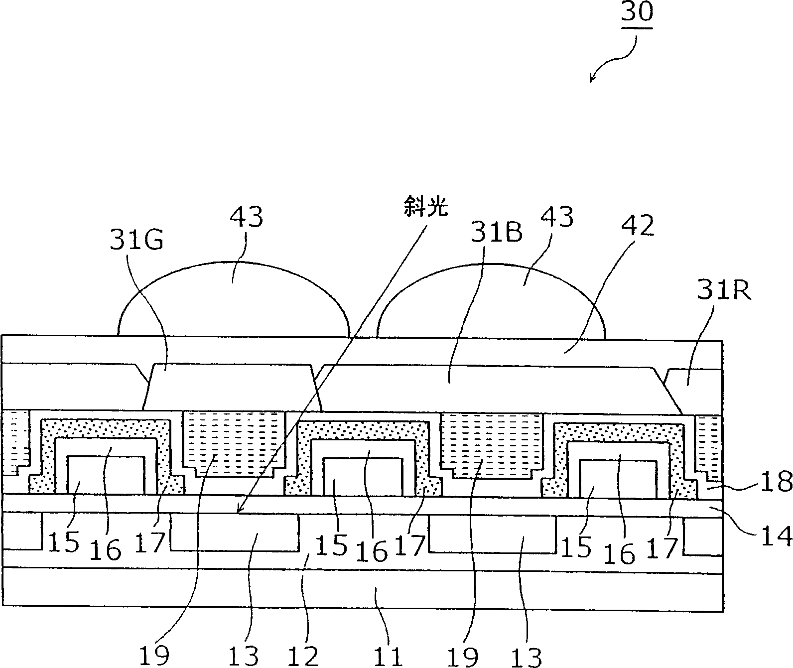
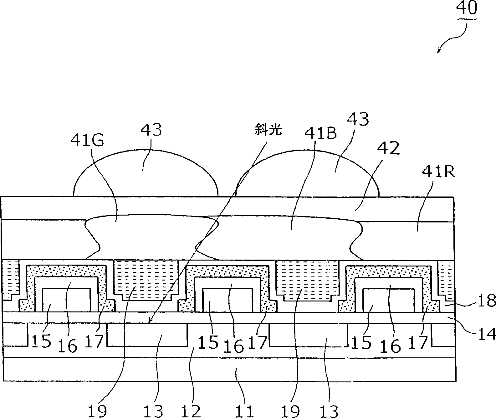
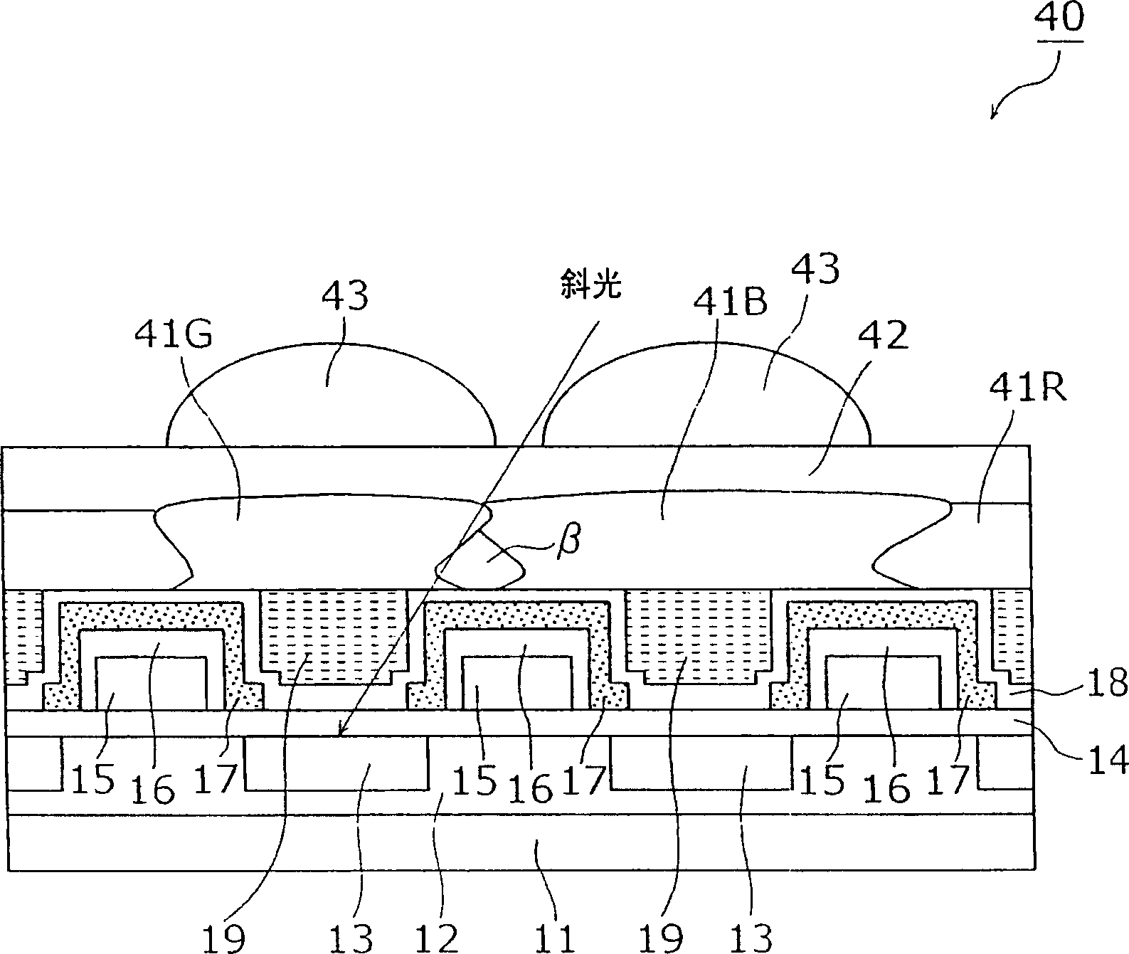
[0058] Figure 4 is a diagram showing a cross-sectional structure of a solid-state imaging device according to an embodiment of the present invention. In addition, this figure shows cross-sections of two photoelectric conversion elements.

[0059] The solid-state imaging device 1 such as Figure 4 As shown, it includes: a semiconductor substrate (N-type semiconductor substrate) 11 of the first conductivity type (for example, N type), a first semiconductor well (P well layer) 12 of the second conductivity type (P type), a plurality of Photoelectric conversion element 13, gate insulating film 14, transfer electrode 15, interlayer insulating film 16, light shielding film 17, surface protection film 18, first transparent planarizing film 19, resin portion 20, color filter layer 21, second transparent flattening film Chemical film 22 and micro lens 23 etc.

[0060] On the surface of the N-type semiconductor substrate 11, a P-well layer 12 having characteristics opposite to those...


PUM


Abstract

To provide a solid-state imaging device capable of improving color mixing, line shading, and sensitivity errors from adjacent color filter layers. It is a solid-state imaging device (1) in which a plurality of pixels having a photoelectric conversion element (13) and a color filter layer (21) formed on the photoelectric conversion element (13) are arranged in a matrix on a semiconductor substrate (11). ), in addition, on the boundary area with the adjacent photoelectric conversion element (13), there is a resin portion (20) formed protruding from the formation surface, and each color filter layer (21) is formed on the adjacent resin portion (20) ), the film thickness of each color filter layer (21) in the peripheral portion corresponding to the top portion is formed thinner than that in the central portion.

Description

technical field [0001] The present invention relates to a solid-state imaging device having a monolithically integrated color filter layer and a method of manufacturing the same. Background technique [0002] In recent years, with the development of image colorization, single-board color solid-state imaging devices, digital still image cameras centered on CCD (charge-coupled device) types, and mobile phones with cameras centered on CMOS types The use of them is rapidly increasing, and the requirements for miniaturization and high pixelation of solid-state imaging devices with monolithic integrated color filters are also increasing. However, due to the demand for such solid-state imaging devices, the light-receiving area of ​​the photoelectric conversion element serving as the light-receiving sensor portion has been reduced. As a result, the photoelectric conversion characteristics (photosensitivity), which are the main characteristics of the solid-state imaging device, have ...

Claims


Application Information

Patent Timeline
IPC IPC(8): H01L27/14G02B5/20
CPCH01L27/14621H01L27/14623H01L27/14625H01L27/14627H01L27/14632H01L27/14685H01L27/14687H01L27/14868
Inventor 横泽贤二
Owner PANASONIC CORP
Why Eureka
Try Eureka