Wafer testing device and method with automatic reversion function

A technology of automatic reply and wafer testing, which is applied in the direction of semiconductor/solid-state device testing/measurement, etc., can solve problems such as low production efficiency, increased production cost, and extended testing time, so as to reduce the overall process time and cost and improve production. efficiency effect

Inactive Publication Date: 2006-05-03
POWERCHIP SEMICON CORP
View PDF0 Cites 10 Cited by
  • Summary
  • Abstract
  • Description
  • Claims
  • Application Information

AI Technical Summary

Problems solved by technology

In this way, the action of repeating the test due to data loss may cause the die to be damaged after repeated tests, and the reset of the t...

Method used


Image

  • Wafer testing device and method with automatic reversion function
  • Wafer testing device and method with automatic reversion function

Examples


Embodiment Construction

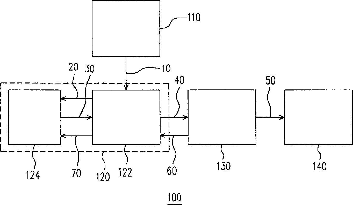
[0041] The wafer testing device and wafer testing method with automatic recovery function of the present invention are suitable for performing operations such as wafer needle testing, laser repairing or final testing in the semiconductor process on a plurality of dies on the wafer.

[0042] Please refer to figure 1 , which shows a schematic view of the wafer testing device with automatic recovery function of the present invention. The wafer testing device 100 includes, for example, a host system 110, a test system (tester) 120, a real-time access module 130, and a database 140, wherein the host system 110 is, for example, a process control system (Manufacturing Execution System, MES), which is It is used to control the overall wafer testing process, including parameters such as wafer movement, process type, wafer batch number, wafer serial number, and process time.

[0043] please refer again figure 1, the test system 120 includes, for example, a control module 122 and a tes...


PUM


Abstract

The invention relates to a crystal sheet measuring device with reset function and the measuring method. The crystal sheet measuring device comprises a host machine system, a measuring system and an immediate access module. The host machine system is used to control the process of the integer measurement; the measuring system is electric connected with the host machine system and is used to receive the order of the host machine system to measure the plurality of crystals and output the measuring data. The immediate access module is electric connected with the measuring device and is used to record the measuring data. When the measuring has been interrupted, the measuring system generates an automatic reset data by the measuring data of immediate access module and measures the crystal by the automatic reset data.

Description

technical field [0001] The invention relates to a wafer testing device and a wafer testing method, and in particular to a wafer testing device and a wafer testing method with an automatic recovery function. Background technique [0002] In today's highly information-based society, the market for multimedia applications continues to expand rapidly, and at the same time drives the development of electronic devices towards the trend of digitalization, networking, regional connection and user-friendly use. In order to meet the above requirements, it is necessary to strengthen the requirements of high-speed processing, multi-function, accumulation, small size, light weight and low price of integrated circuit (Integrated Circuits, IC) components, so the semiconductor process is also moving towards miniature and high-density development. In the semiconductor industry, the production of integrated circuits is mainly divided into three stages: the manufacture of wafers, the manufact...

Claims


Application Information

Patent Timeline
IPC IPC(8): H01L21/66
Inventor 吴秋萍林修民
Owner POWERCHIP SEMICON CORP
Why Eureka
Try Eureka