Electromagnetic wave absorbing material

A technology for absorbing materials and electromagnetic waves, applied in electrical components, magnetic field/electric field shielding, other chemical processes, etc., can solve the problems of difficulty in taking into account wave impedance matching, lack of electromagnetic wave absorbers, etc., to prevent electromagnetic wave pollution, wide application prospects, The effect of good absorbing properties

Inactive Publication Date: 2006-05-03
ZHEJIANG UNIV OF TECH
View PDF0 Cites 32 Cited by
  • Summary
  • Abstract
  • Description
  • Claims
  • Application Information

AI Technical Summary

Problems solved by technology

Compared with multi-layer structures, single-layer structure absorbing materials have the advantages of one-time molding, convenient construction, light weight, and thin thickness. However, there is currently a lack of systematic

Method used


Image

  • Electromagnetic wave absorbing material
  • Electromagnetic wave absorbing material
  • Electromagnetic wave absorbing material

Examples


Embodiment 1

[0020] Materials used in this embodiment: high-density polyethylene (HDPE) and isotactic polypropylene (iPP) are selected as the polymer, and conductive carbon black (CB) is selected as the electromagnetic wave absorber.

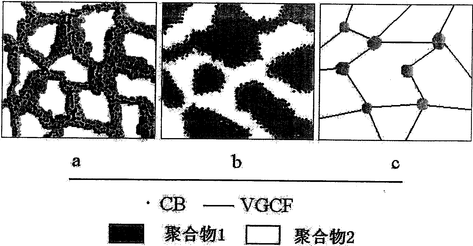
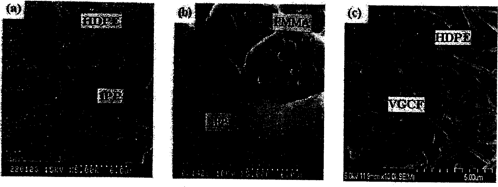
[0021] First use a two-roll mill, knead 50g of HDPE and 50g of iPP at 160°C for 5 minutes, then add 5g of CB and knead for 5 minutes, then mold at a pressure of 19.6MPa for 5 minutes, and then quench into water , to obtain a wave-absorbing sheet with a thickness of 2 mm. The phase structure of the material is as figure 1 as shown in a. From SEM figure 2 As can be seen from a, CB is selectively enriched in the HDPE phase.

Embodiment 2

[0023] Materials used in this embodiment: polymethyl methacrylate (PMMA) and isotactic polypropylene (iPP) are selected as polymers, and conductive carbon black (CB) is selected as electromagnetic wave absorber.

[0024] First use a two-roll mill, knead 50g of PMMA and 50g of iPP at 180°C for 5 minutes, then add 5g of CB and knead for 5 minutes, then mold at a pressure of 19.6MPa for 5 minutes, and then quench into water , to obtain a wave-absorbing sheet with a thickness of 2 mm. The phase structure of the material is as figure 1 as shown in b. From SEM figure 2 It can be seen from b that CB is selectively enriched at the interface of PMMA and iPP.

Embodiment 3

[0026] Materials used in this embodiment: high-density polyethylene (HDPE) and polymethyl methacrylate (PMMA) are selected as polymers, and vapor grown carbon fibers (VGCF) are selected as electromagnetic wave absorbers. First use a two-roll mill, knead 5g of HDPE and 95g of PMMA at 180°C for 5 minutes, then add 5g of VGCF and knead for 5 minutes, then mold at a pressure of 19.6MPa for 5 minutes, and then quench into water , to obtain a wave-absorbing sheet with a thickness of 2 mm. In order to obtain a clear picture of the phase structure, the sample was extracted with chloroform for 72 hours, and the PMMA was dissolved to obtain a mixture of HDPE / VGCF. The phase structure of the material is as figure 1 as shown in c. From SEM figure 2 It can be seen from c that HDPE bonds VGCF together like a "rivet" to form a network frame structure.


PUM

PropertyMeasurementUnit
Thicknessaaaaaaaaaa

Abstract

This invention relates to an electromagnetic wave absorption material, which is a high molecular compound material compounded by mixing a polymer matrix of two phases or more than two and an electromagnetic wave absorbent, in which, the polymer matrix is composed of two or more than two kinds of incompatible polymers and the material has fine wave absorption performance.

Description

(1) Technical field [0001] The invention relates to an electromagnetic wave absorbing material, in particular to a polymer-based single-layer electromagnetic wave absorbing material with adjustable phase structure. (2) Background technology [0002] For electromagnetic wave absorbing materials, a single electromagnetic wave absorber has a narrow absorbing frequency band and cannot solve the problem of non-reflection. Considering the size and mechanical properties of the material, it is generally used in the form of electromagnetic wave absorbers for multi-component compounding. The design of electromagnetic wave absorbing composite materials usually mainly solves the following two problems: one is how to make more electromagnetic waves enter the interior of the material instead of reflecting back from the surface, that is, wave impedance matching must be considered; The electromagnetic wave is absorbed to the maximum in the medium, that is, the electromagnetic loss efficienc...

Claims


Application Information

Patent Timeline
IPC IPC(8): H05K9/00C09K3/00
Inventor 张诚王平
Owner ZHEJIANG UNIV OF TECH
Why Eureka
Try Eureka