Transistor array substrate and display panel

A transistor array and display panel technology, applied in static indicators, lighting devices, light sources, etc., can solve problems such as wiring current flow delay, transistor characteristic change, voltage drop, etc., and achieve the effect of suppressing signal delay and voltage drop.

Inactive Publication Date: 2006-05-10
SOLAS OLED LTD
View PDF1 Cites 7 Cited by
  • Summary
  • Abstract
  • Description
  • Claims
  • Application Information

AI Technical Summary

Problems solved by technology

[0006] However, since the electrode of the thin film transistor is designed on the premise that it is used as a transistor, in other words, it is not designed on the premise that a current flows through the light-emitting element, so it is a thin film as its name suggests. When current flows through the element, a voltage drop occurs due to the resistance of the wiring, causing a delay in the flow of current through the wiring.
In order to suppress voltage drop and current delay, it is desirable to reduce the resistance of the wiring. However, for this purpose, the metal layer constituting the source and drain electrodes of the transistor or the metal layer constituting the gate electrode must be thickened, or a sufficient current flow When laying out these metal layers to form a low-resistance wiring, the overlapping area of ​​the wiring and other wiring or conductors increases when viewed from above, and parasitic capacitance is generated during this period, which causes a delay in the flow of current. In the case of a so-called bottom emission structure that emits EL light from the side, the wiring blocks the light emitted from the EL element, so the numerical aperture, which is a ratio of the light emitting area, becomes small
In addition, if the gate electrode of the thin film transistor is thickened for low resistance, it is necessary to thicken the planarizing film to planarize the level of the gate electrode (for example, when the thin film transistor has an inverted staggered structure (reverse stagger structure). In this case, equivalent to the gate insulating film), the characteristics of the transistor may be greatly changed. In addition, if the source and drain electrodes are thickened, the etching accuracy of the source and drain electrodes may decrease, so there may be a problem with the transistor. bad influence

Method used


Image

  • Transistor array substrate and display panel
  • Transistor array substrate and display panel
  • Transistor array substrate and display panel

Examples


no. 1 Embodiment approach

[0071] Hereinafter, embodiments for carrying out the present invention will be described with reference to the drawings. However, in the following embodiments, it is preferable to add various limitations technically in order to implement the present invention, but the scope of the invention is not limited to the following embodiments and illustrations.

[0072] [Overall configuration of EL display panel]

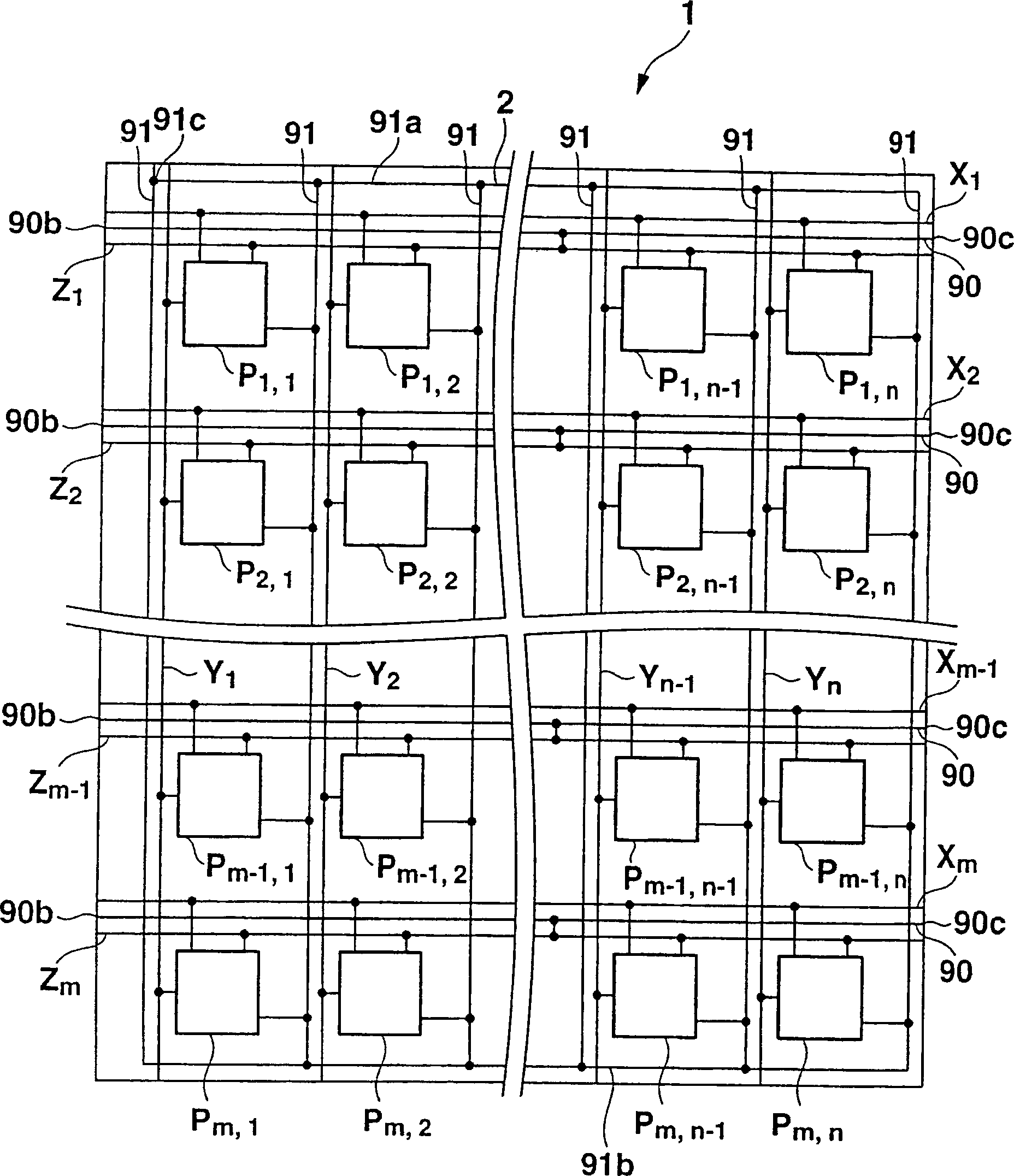
[0073] figure 1 A schematic diagram of an EL display panel 1 of an active matrix driving method is shown in . like figure 1 As shown, the EL display panel 1 has a light-transmitting flexible sheet-shaped or rigid plate-shaped insulating substrate 2; n (multiple) signal lines Y arranged parallel to each other on the insulating substrate 2 1 -Y n ; When looking down on the insulating substrate 2 and the signal line Y 1 -Y n m (multiple) scanning lines X arranged orthogonally on the insulating substrate 2 1 -X m ; at scan line X 1 -X m Between each and scan line X 1 ...

no. 2 Embodiment approach

[0189] [Overall configuration of EL display panel]

[0190] Figure 20 A schematic diagram of an EL display panel 1 of an active matrix driving method is shown in . like Figure 20 As shown, the EL display panel 1 has a light-transmitting flexible sheet-shaped or rigid plate-shaped insulating substrate 2; n (multiple) signal lines Y arranged parallel to each other on the insulating substrate 2 1 -Y n ; Insulating substrate 2, relative to signal line Y when viewed from above 1 -Y n m (multiple) scanning lines X arranged orthogonally on the insulating substrate 2 1 -X m ; at each scan line X 1 -X m Between and scan line X 1 -X m m (multiple) supply lines Z arranged in parallel and differently from each other on the insulating substrate 2 1 -Z m ; along signal line Y 1 -Y n and scanline X 1 -X m (m×n) groups of pixel circuits P arranged in a matrix on the insulating substrate 2 1,1 -P m,n ;connected to the supply line Z 1 -Z m And the signal line Y relative to...

Deformed example 1

[0243] In addition, the present invention is not limited to the above-described embodiments, and various improvements and design changes can be made without departing from the spirit of the present invention.

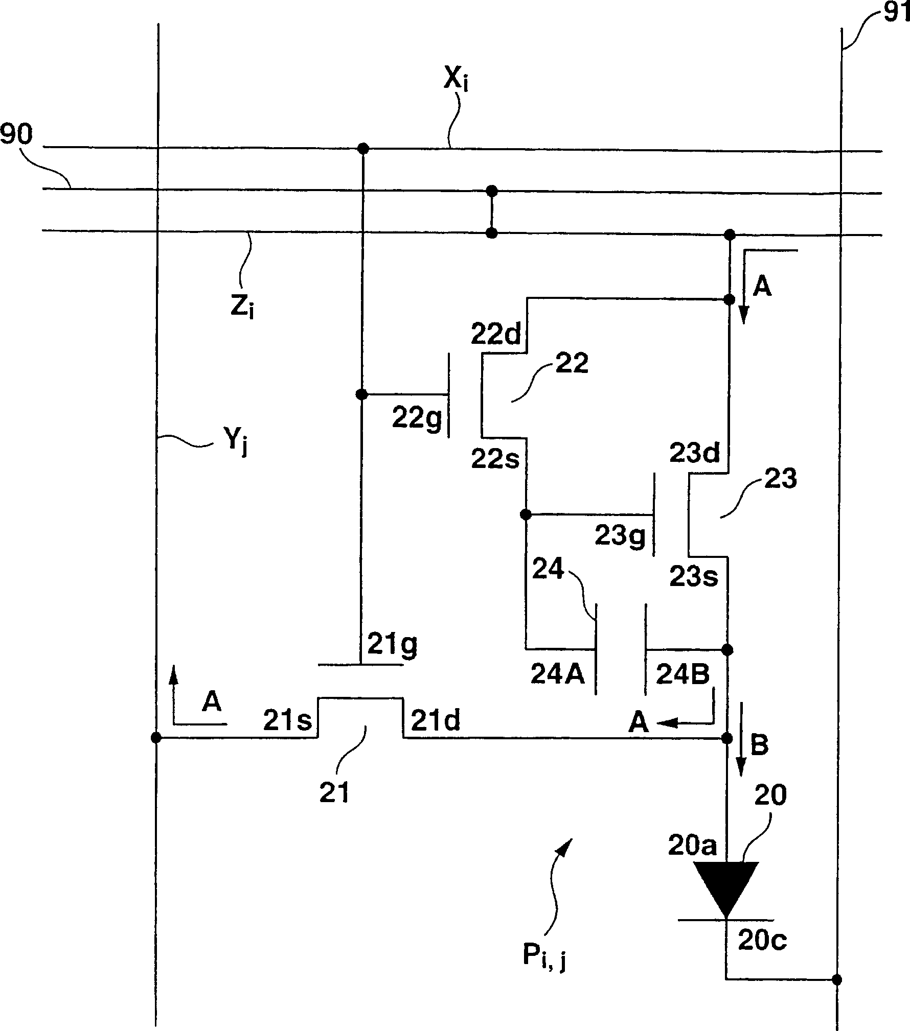
[0244] In addition, in the above-described embodiment, the transistors 21 to 23 have been described as N-channel type field effect transistors. Transistors 21-23 may also be P-channel type field effect transistors. At this time, at figure 2 In the circuit configuration of , the relationship between the sources 21s, 22s, and 23s of the transistors 21-23 and the drains 21d, 22d, and 23d of the transistors 21-23 is reversed. For example, when the driving transistor 23 is a P-channel type field effect transistor, the drain 23d of the driving transistor 23 is connected to the pixel electrode 20a of the organic EL element 20, and the source 23s is connected to the supply line Z. i conduction.


PUM

PropertyMeasurementUnit
Film thicknessaaaaaaaaaa
Widthaaaaaaaaaa
Resistivityaaaaaaaaaa

Abstract

The transistor array substrate of the present invention reduces the voltage drop of wiring. The transistor array substrate includes: a substrate; a plurality of driving transistors arranged in a matrix on the substrate, and a gate insulating film is sandwiched between the gate, the source, and the drain; a plurality of signal lines connected to the The gates of a plurality of drive transistors are laid out together and arranged to extend in a predetermined direction on the substrate; a plurality of supply lines are laid out together with the sources and drains of the drive transistors, and are arranged across the gates. The electrode insulating film is arranged crosswise with the plurality of signal lines, and conducts with one of the source and drain of the driving transistor; a plurality of power supply wirings are respectively stacked on the plurality of supply lines along the plurality of supply lines .

Description

technical field [0001] The present invention relates to a transistor array substrate including transistors, and a display panel using a light emitting element that emits light by passing a current through the transistor array substrate. Background technique [0002] Organic electroluminescent display panels can be roughly divided into two types: passive drive mode and active matrix drive mode, but organic electroluminescent display panels with active matrix drive mode are better than passive drive modes in terms of high contrast and high definition. . For example, in the conventional organic electroluminescent display panel of the active matrix driving method described in Patent Document 1, an organic electroluminescent element (hereinafter referred to as an organic EL element), an organic electroluminescent element (hereinafter referred to as an organic EL element), a gate A drive transistor that applies a voltage signal corresponding to image data to the organic EL elemen...

Claims


Application Information

Patent Timeline
IPC IPC(8): G09G3/30H05B33/12
Inventor 下田悟白崎友之小仓润熊谷稔
Owner SOLAS OLED LTD
Why Eureka
Try Eureka