
FPGA logic unit functional model and universal logic unit containing computing method

A logic unit and functional model technology, applied in computing, special data processing applications, instruments, etc., can solve the problems of wasting layout area, unoptimized application fields, and no logical unit function model

Inactive Publication Date: 2006-06-14
FUDAN UNIV
View PDF0 Cites 11 Cited by
  • Summary
  • Abstract
  • Description
  • Claims
  • Application Information

AI Technical Summary

Problems solved by technology

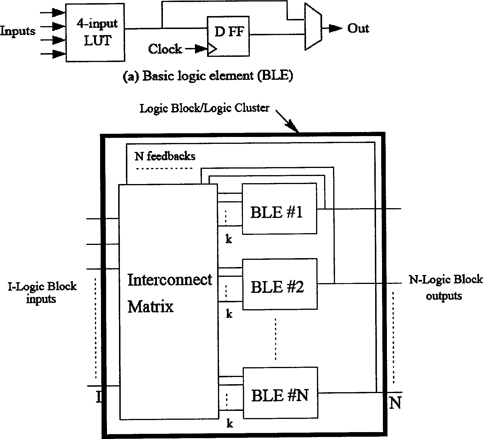
Logic cluster is the simplest structural model of hierarchical logic blocks. Its internal logic unit BLE and internal interconnection switch matrix adopt the most simplified method. Its shortcomings are: first, the logic unit BLE structure It is the simplest structure that can realize combinatorial and sequential logic. It has simple functions and does not contain any special functional elements, so it is not optimized for the actual application field of FPGA; second, the internal interconnection switch matrix is ​​fully connected, so it is very waste of layout area
The reason is that for different logical unit structures, there is no good general functional model of logical units

Method used


Image

  • FPGA logic unit functional model and universal logic unit containing computing method
  • FPGA logic unit functional model and universal logic unit containing computing method
  • FPGA logic unit functional model and universal logic unit containing computing method

Examples


Embodiment Construction

[0155] Figure 4 It is the logic unit structure diagram of Xilinx XC4000 series FPGA. It is difficult to directly see its logic functions from the diagram. Follow the steps below to model its functions.

[0156] (a) Extraction of functional elements and switch multiplexers.

[0157] The functional element has two 4-input LUTs, one 3-input LUT, two D flip-flops, and multiple switch multiplexers (controlled by programming points R1-R10). see programming Figure 13 Callouts in .

[0158] (2) Describe the logical unit structure.

[0159] The logic unit of XC4000 is formed by connecting these functional components and switch multiplexers in (1). can be described by verilog HDL Figure 13 logical unit structure.

[0160] (3) Configure the values ​​of the programming points to obtain a series of functional circuits.

[0161] Figure 14 It shows the functional circuit obtained by the logic unit of XC4000 under the value of programming point R1 ~ R10 = 0010101111. See Table 1 ...


PUM


Abstract

The invention belongs to the field of electronic design automation technique, concretely a functional model of FPGA logic cells and a universal logic cell packing algorithm. The model firstly extracts functional components from the FPGA logic cells, then using the connection of the functional components and multi-channel switch selectors to describe the whole structure of logic cells, successively making different configurations on the logic cells to generate many available functional circuits formed only by connection of logic cells and the model can widely describe the structure of logic cells of the existing FPGAs and obtain all logic functions of logic cells by their corresponding available functional circuits. Based on the functional model of FPGA logic cells, the invention advances a universal logic cell packing algorithmí¬FDUPack whose kernel idea is to repeatedly make circuit diagram mode matching on each available functional circuit in the user circuit and which is a universal algorithm of processing various logic cell packing problems.

Description

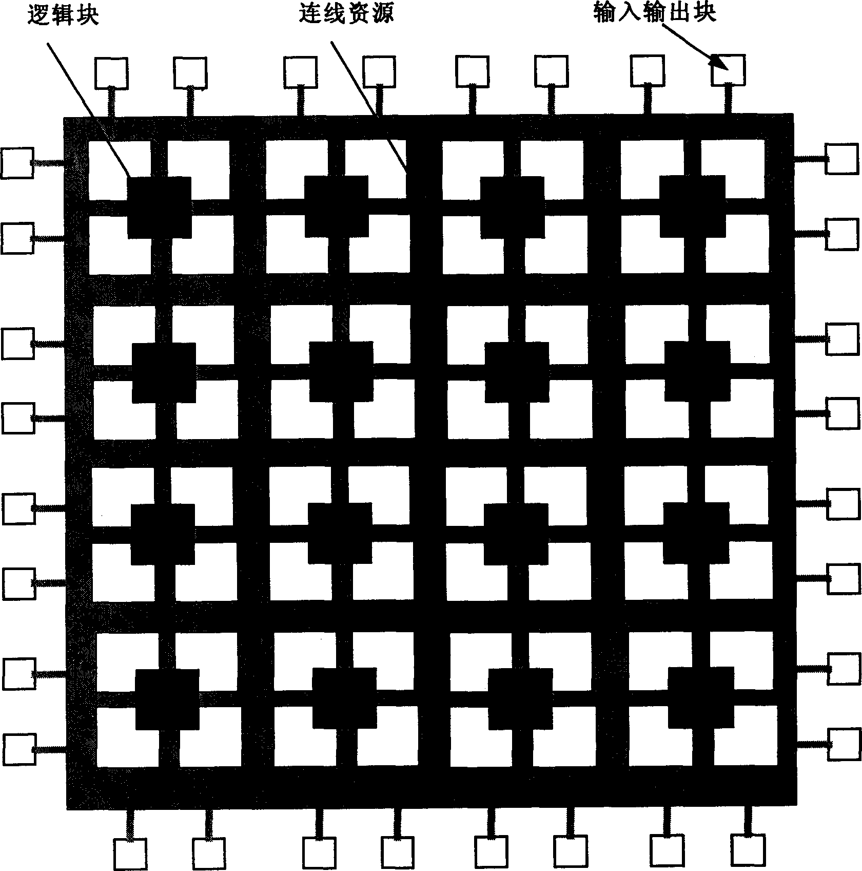
technical field [0001] The invention belongs to the technical field of electronic design automation (Electronic Design Automation, EDA), and in particular relates to a functional model of an FPGA logic unit and a general logic unit packing algorithm. technical background [0002] Literature [1] points out that a logic block (Logic block) is a component that implements user circuit logic in a Field Programmable Gate Array (Filed Programmable Logic Array, FPGA). Oblock) is the three major components of FPGA, such as figure 1 shown. [0003] Logical blocks can be divided into flat logical blocks (also known as logical units, excluding internal interconnections) and hierarchical logical blocks (also known as cluster-structured logical blocks, which contain multiple logical units and internal interconnection resources). interconnect switch matrix). With the development of FPGA structure, hierarchical logic blocks have gradually replaced planar logic blocks and become the mains...

Claims


Application Information

Patent Timeline
IPC IPC(8): G06F17/50
Inventor 童家榕倪刚来金梅
Owner FUDAN UNIV
Learn More