

Silicon micro piezoelectric sensor chip and its preparing method
A sensor chip, micro-piezoelectric technology, applied in the direction of piezoelectric devices/electrostrictive devices, electrical components, impedance networks, etc., can solve the problems of reducing the sensitivity and yield of micro-sensors, the decrease of sensor sensitivity, and the stress of vibrating membrane. , to achieve the effect of reducing corrosion defects, reducing stress inhomogeneity, and fast corrosion speed
- Summary
- Abstract
- Description
- Claims
- Application Information
AI Technical Summary
Problems solved by technology
Method used
Image

Examples
Embodiment 1
[0047] Embodiment 1, using the preparation method of the present invention to prepare a novel piezoelectric sensor chip, the steps are as follows:
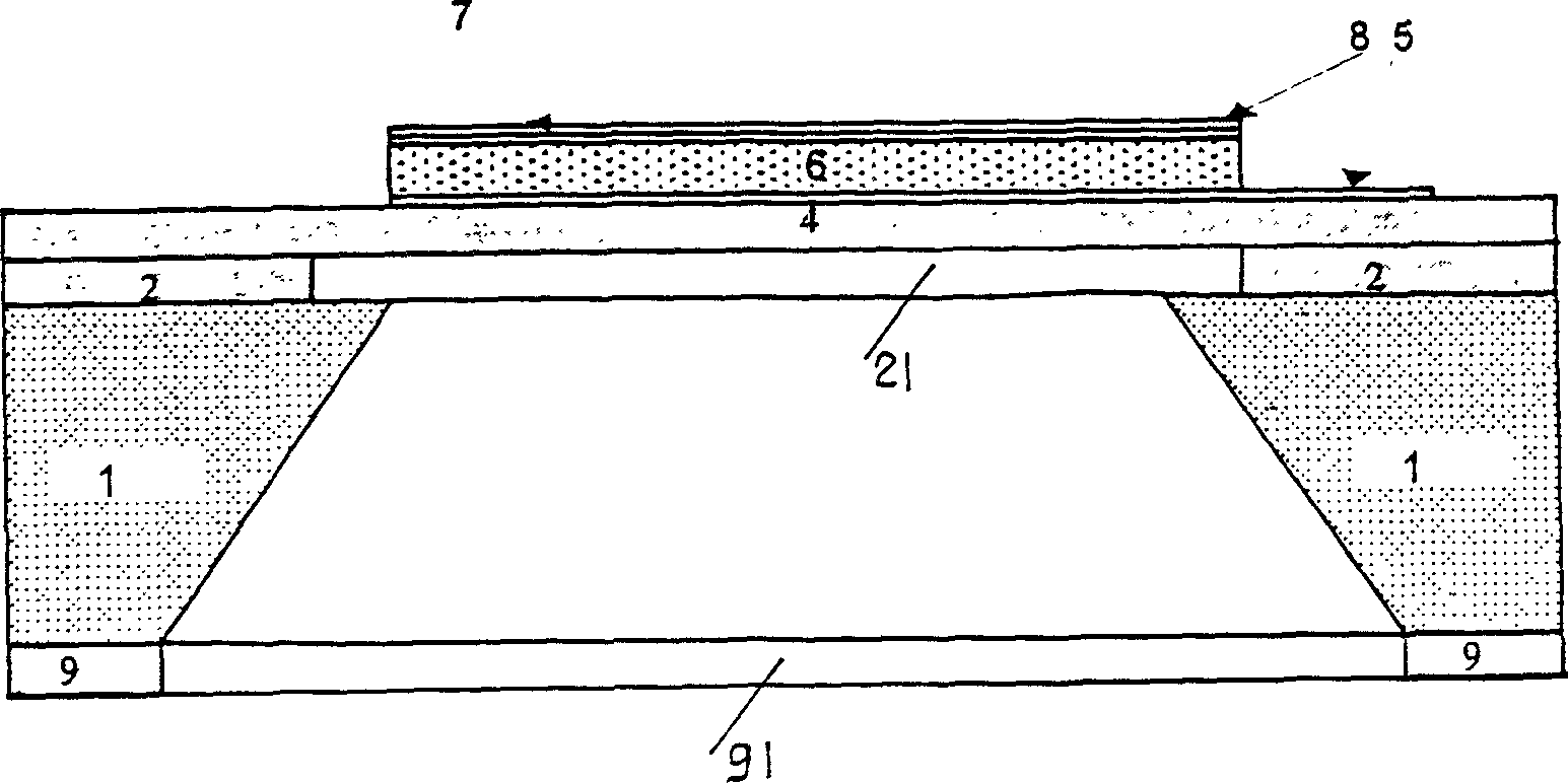
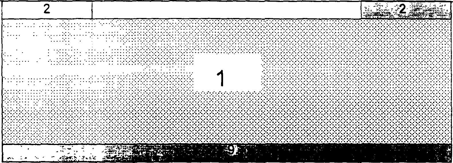
[0048] 1) Clean n-type silicon substrate 1
[0049] Cleaning the n-type silicon substrate 1 with an acid cleaning solution and an alkaline cleaning solution respectively, and then rinsing it with deionized water;
[0050] 2) On the front and back surfaces of the n-type silicon substrate 1, respectively deposit a silicon nitride base film layer 2 with a thickness of 0.2 μm and a silicon nitride mask layer 9 with a thickness of 0.2 μm by using a low-pressure chemical vapor deposition equipment ;
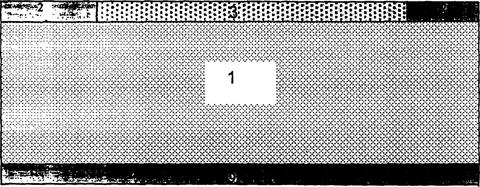
[0051] 3) Preparation of zinc oxide sacrificial layer 3
[0052] Coating a positive photoresist on the surface of the silicon nitride base film layer 2, and exposing by photolithography to form a circular sacrificial layer inverted film photolithographic pattern;
[0053] Then use a high-density plasma etching machine to photoetch the sil...
Embodiment 2
[0067] Embodiment 2, using the preparation method of the present invention to prepare a novel piezoelectric sensor chip, the steps are as follows:
[0068] 1) Clean n-type silicon substrate 1
[0069] Cleaning the n-type silicon substrate 1 with an acid cleaning solution and an alkaline cleaning solution respectively, and then rinsing it with deionized water;
[0070] 2) On the front and back surfaces of the n-type silicon substrate 1, respectively deposit a silicon nitride base film layer 2 with a thickness of 2 μm and a silicon nitride mask layer 9 with a thickness of 2 μm by using low-pressure chemical vapor deposition equipment;
[0071] 3) Preparation of phosphosilicate glass sacrificial layer 3
[0072] Coating a positive photoresist on the surface of the silicon nitride base film layer 2, and exposing by photolithography to form a circular sacrificial layer inverted film photolithographic pattern;
[0073] Then use a high-density plasma etching machine to photoetch th...
Embodiment 3
[0087] Embodiment 3, using the preparation method of the present invention to prepare a novel piezoelectric sensor chip, the steps are as follows:
[0088] 1) Clean n-type silicon substrate 1
[0089] Cleaning the n-type silicon substrate 1 with an acid cleaning solution and an alkaline cleaning solution respectively, and then rinsing it with deionized water;
[0090] 2) On the front and back surfaces of the n-type silicon substrate 1, respectively deposit a silicon nitride base film layer 2 with a thickness of 1 μm and a silicon nitride mask layer 9 with a thickness of 1 μm by using low-pressure chemical vapor deposition equipment;
[0091] 3) Preparation of zinc oxide sacrificial layer 3
[0092] Coating a positive photoresist on the surface of the silicon nitride base film layer 2, and exposing by photolithography to form a circular sacrificial layer inverted film photolithographic pattern;
[0093] Then use a high-density plasma etching machine to photoetch the silicon n...
PUM
| Property | Measurement | Unit |
|---|---|---|
| Thickness | aaaaa | aaaaa |
| Thickness | aaaaa | aaaaa |
| Thickness | aaaaa | aaaaa |
Abstract
Description
Claims
Application Information