Silicon micro condenser microphone chip and its preparing method

A condenser microphone and silicon micro technology, applied in the direction of electrostatic transducer microphones, sensors, electrical components, etc., can solve the problems of large influence, long time consumption, high cost of silicon micro capacitor microphone chip, etc., achieve simple and easy process, overcome problems and difficult effects

Inactive Publication Date: 2006-06-21
INST OF ACOUSTICS CHINESE ACAD OF SCI
View PDF2 Cites 18 Cited by
  • Summary
  • Abstract
  • Description
  • Claims
  • Application Information

AI Technical Summary

Problems solved by technology

The deep boron diffusion takes a long time (generally more than 20 hours), and the deep boron diffusion causes the silicon substrate to warp at the edge, making it difficult to manufacture various processes after the deep boron diffusion
In particular, large silicon substrates (such as 4-inch or larger substrates) for production are greatly affected
[0008] 3) Due to the anisotropy of silicon itself in the etching solution, for silicon microcapacitor sound transmission chips, the thickness of the backplane is required to be between 12 microns and 20 microns. In this way, the backplane prepared with deep concentrated boron diffusion The perforation cannot be too small, therefore, the size of the silicon microcapacitor microphone chip cannot be too small, which makes the cost of the silicon microcapacitor microphone chip relatively high during mass production

Method used


Image

  • Silicon micro condenser microphone chip and its preparing method
  • Silicon micro condenser microphone chip and its preparing method
  • Silicon micro condenser microphone chip and its preparing method

Examples


Embodiment 1

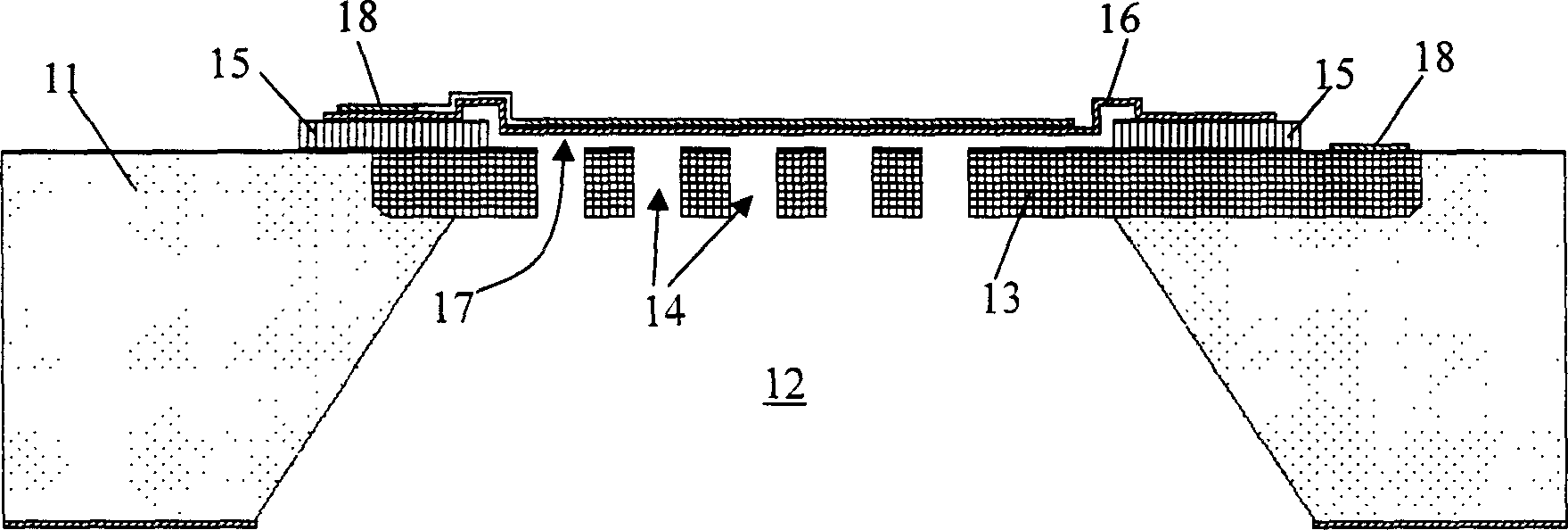
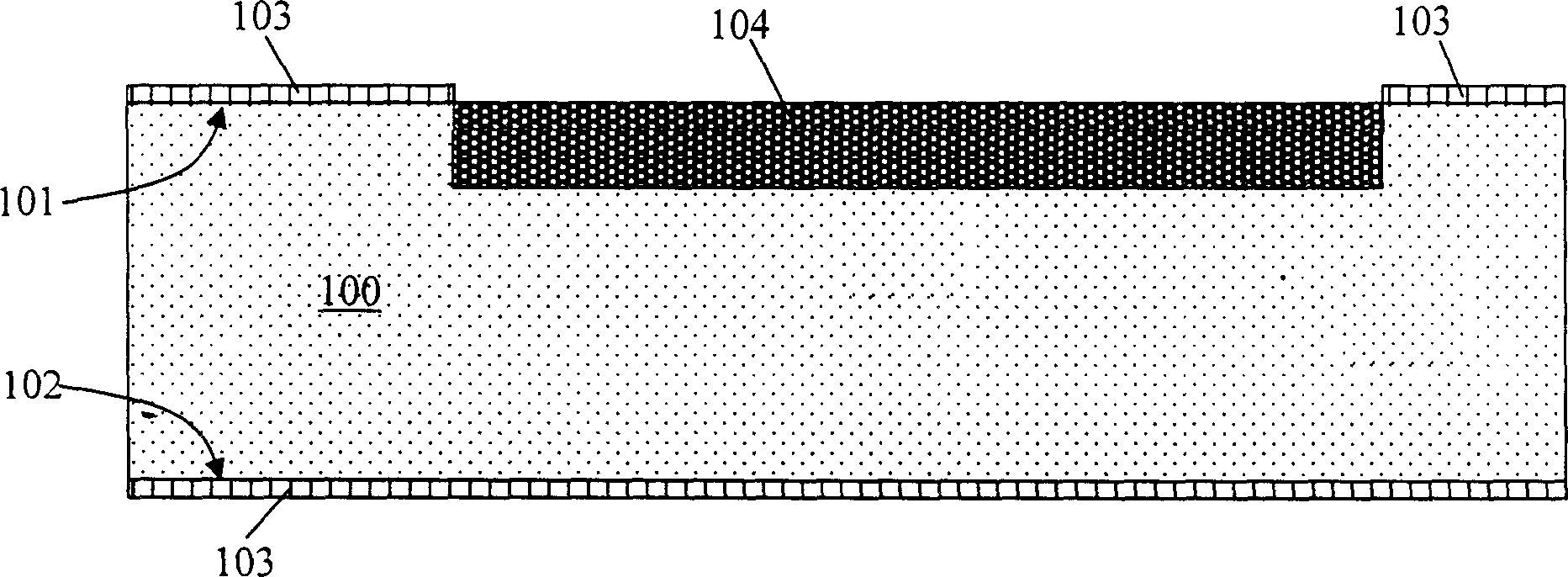
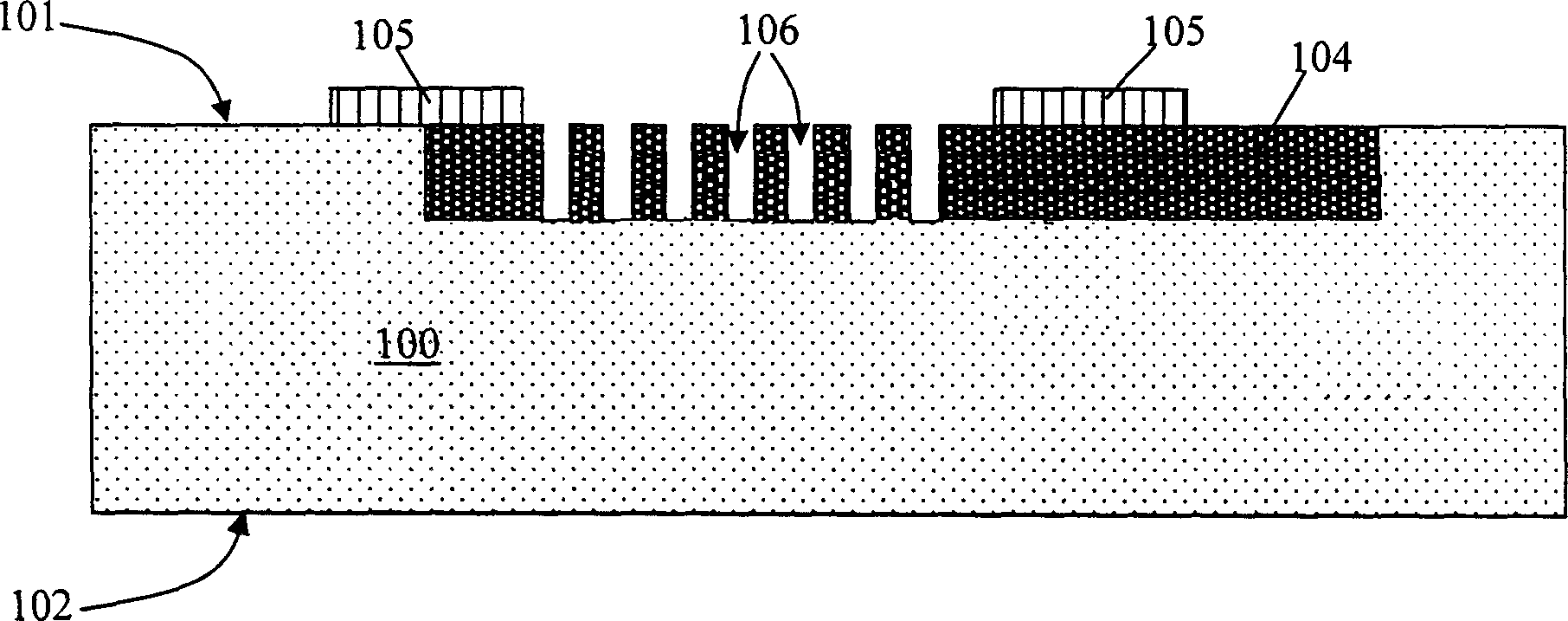
[0039] figure 2 ~ Fig. 5 shows the preparation process of the silicon microcapacitance microphone chip of the present invention in one embodiment, wherein Fig. 5 shows the prepared microphone chip according to the method of the present invention.

[0040] Such as figure 2 As shown, a silicon substrate 100 is selected first, and the silicon substrate 100 can be an n-type or p+ type silicon wafer. The silicon substrate 100 has an upper surface 101 and a lower surface 102. In one embodiment, the thickness of the silicon substrate 100 is 400 micrometers, but it can be understood that those skilled in the art can adjust the thickness of the silicon substrate 100 according to the required microphone chip size. Silicon substrates 100 with different thicknesses are selected. A layer of high-temperature silicon dioxide is grown on the silicon substrate 100 through a high-temperature oxidation process. Exemplarily, the thickness of the high-temperature silicon dioxide is 1 micron; Af...

Embodiment 2

[0046] Figure 7 ~ Figure 10 Show the preparation process of the silicon microcapacitance microphone chip of the present invention in another embodiment, wherein Figure 10 In this example a good microphone chip was prepared according to the method of the present invention. In the following description of embodiment 2, the same part as embodiment 1 will not be described again, and the difference between embodiment 2 and embodiment 1 will be described emphatically, wherein, in Figure 7 ~ Figure 10 In, the composition identical with embodiment 1 still uses and figure 2 The same reference numerals as in FIG. 5 and different reference numerals are used for parts different from those in Embodiment 1. FIG.

[0047] Such as Figure 7 As shown, the difference between this embodiment and Embodiment 1 is that the thickness of the doped layer 204 is significantly smaller than figure 2 The thickness of the middle doped layer 104 . It can be known from the following description tha...


PUM

PropertyMeasurementUnit
thicknessaaaaaaaaaa

Abstract

The invention discloses a silicon micro-condenser microphone chip, which comprises a silicon substrate with a perforated back board on top. Wherein, the said back board comprises a continual doping layer on top of said substrate with a plurality of acoustics holes by etching the continual doping layer or also a silicon material layer under the doping layer. This invention overcomes the problem to prepare back board and perforation with deep-selective enriched boron, and provides a simple and practical technique for industrial production.

Description

technical field [0001] The invention relates to the field of semiconductor devices, in particular to a silicon microcapacitor microphone chip and a preparation method thereof. Background technique [0002] The silicon microcapacitor microphone is a new type of microphone, which usually consists of a silicon chip part and a peripheral circuit part forming a silicon microcapacitor. Among them, the silicon microcapacitor chip part is the core of the microphone, which is manufactured on a silicon substrate through a complex bulk etching process using modern VLSI technology. The silicon microcapacitor chip part is composed of a silicon substrate and a perforated backplane or an acoustic hole backplane, an air gap, an isolation layer, a vibrating film / metal film and a metal electrode. Due to the complexity of its manufacturing process, with the development of technology, many new structures and their preparation methods are constantly being proposed. [0003] It is known that ab...

Claims


Application Information

Patent Timeline
Patent Type & Authority Applications(China)
IPC IPC(8): H04R19/04H04R31/00
Inventor 乔东海田静徐联汪承灏
Owner INST OF ACOUSTICS CHINESE ACAD OF SCI
Why Eureka
Try Eureka