Voltage boost circuit

A technology of boosting circuit and generating circuit, which is applied in the direction of conversion equipment without intermediate conversion to AC, and achieves the effect of simple circuit, high replacement, and low electromagnetic radiation interference.

Inactive Publication Date: 2006-07-19
齐元国际股份有限公司
View PDF0 Cites 0 Cited by
  • Summary
  • Abstract
  • Description
  • Claims
  • Application Information

AI Technical Summary

Problems solved by technology

At the same time, the present invention can also achieve the effects of cost reduction and easy maintenance.

Method used


Image

  • Voltage boost circuit
  • Voltage boost circuit
  • Voltage boost circuit

Examples


Embodiment Construction

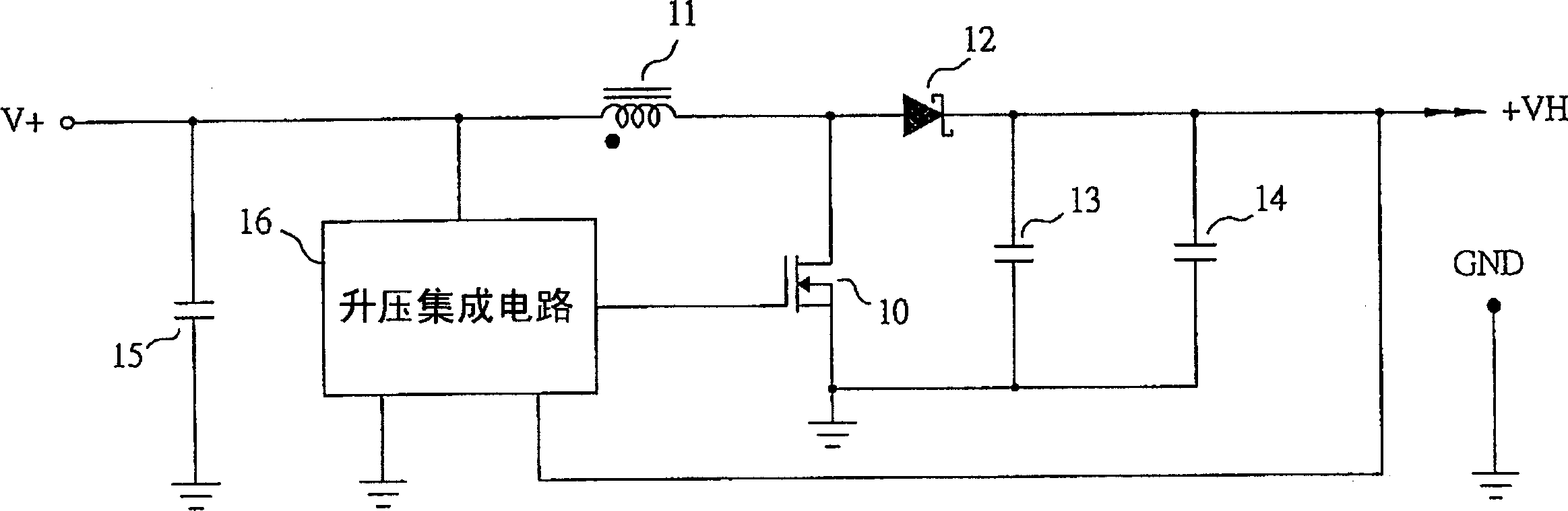
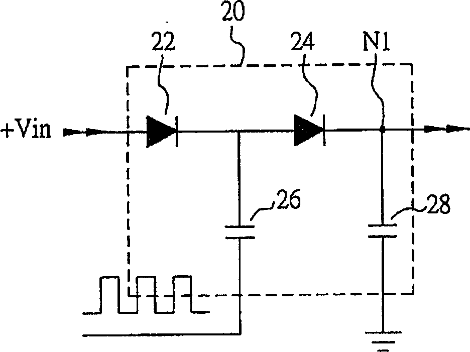
[0024] Figure 2a It is a schematic diagram of a positive voltage boosting circuit according to a preferred embodiment of the present invention. Please refer to Figure 2a , the positive voltage boost circuit includes a voltage boosting block 20, which has a first diode 22, a second diode 24, a first coupling capacitor 26 and a second coupling capacitor 28, wherein the first two One end of the pole tube 22 is used to receive an input positive voltage Vin, and the other end is simultaneously connected to the first coupling capacitor 26 and one end of the second diode 24, the other end of the first coupling capacitor 26 receives the function wave signal, and the second and second diodes The other end of the pole tube is connected to one end of the second coupling capacitor 28 to output a voltage from the node N1, and the other end of the second coupling capacitor 28 is grounded.

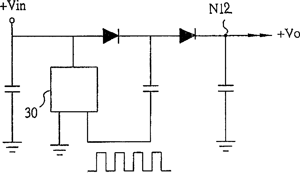
[0025] Figure 2b It is a circuit diagram of a positive voltage boosting circuit according to a ...


PUM


Abstract

The invention relates to a voltage rise circuit, which comprises a voltage rise block and a function wave generating circuit. Wherein, the voltage rise block is formed by the first diode, the second diode, the first coupling capacitor, and the second coupling capacitor to raise the input voltage. The invention can form multistage voltage rise block according to different load voltage, and said voltage rise block can be maintained by changing diode and capacitor, and via increasing / decreasing the matched groups of diode and capacitor to realize the range of voltage rise to reduce time and cost.

Description

technical field [0001] The invention relates to a voltage boosting circuit, and in particular to a voltage boosting circuit using a diode and a capacitor to realize the voltage boosting effect. Background technique [0002] The known step-up circuit (Step-up DC / DC controller IC) realizes positive voltage or negative voltage boost by matching with a circuit composed of transistors or field effect transistors, inductors, Schottky diodes, filter capacitors and the like. Such as figure 1 Shown is a circuit diagram of a known positive voltage boost circuit, which includes a transistor or field effect transistor 10 , an inductor 11 , a Schottky diode 12 , a capacitor 13 , a capacitor 14 , a capacitor 15 and a boost integrated circuit 16 . [0003] The above-mentioned boost circuit has the following disadvantages: the use of inductor charging and discharging effects and high-frequency oscillation results in high-energy electromagnetic radiation interference; if an imported boost i...

Claims


Application Information

Patent Timeline
Patent Type & Authority Applications(China)
IPC IPC(8): H02M3/06
Inventor 吴国全陈敦仁
Owner 齐元国际股份有限公司
Why Eureka
Try Eureka