Voltage boost circuit

A booster circuit and loop technology, applied in the direction of conversion equipment without intermediate conversion to AC, can solve the problems of large loss, large reverse recovery current and reverse recovery time, and the switching frequency cannot be increased any more.

Active Publication Date: 2006-07-19
ZHUZHOU CSR TIMES ELECTRIC CO LTD
View PDF0 Cites 8 Cited by
  • Summary
  • Abstract
  • Description
  • Claims
  • Application Information

AI Technical Summary

Problems solved by technology

The switching frequency is not allowed to increase
[0006] 2 Switch K usually uses IGBT or MOSFET power devices, and each switch will generate corresponding switching losses
Reverse recovery current and reverse recovery time tend to be large, causing large losses and are directly proportional to switching frequency
Due to this factor, the switching frequency increase is limited

Method used


Image

  • Voltage boost circuit
  • Voltage boost circuit
  • Voltage boost circuit

Examples


Embodiment Construction

[0017] The present invention will be further described below in conjunction with the accompanying drawings and embodiments.

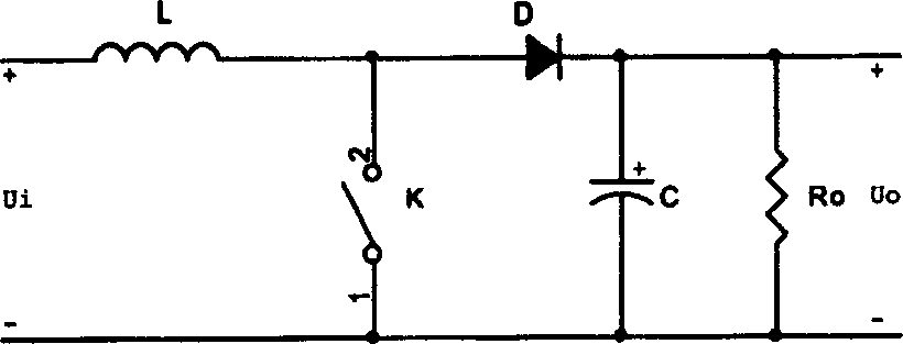
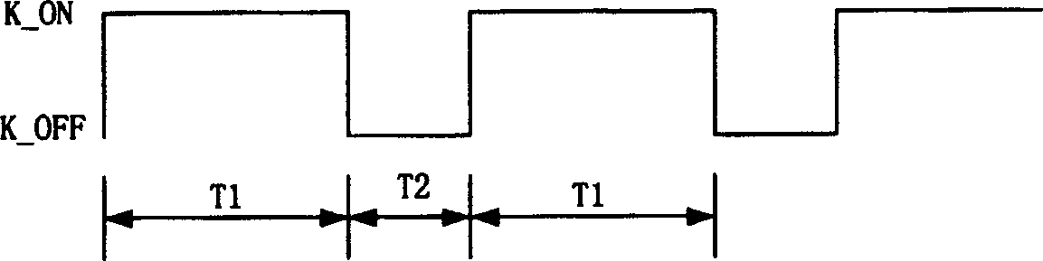
[0018] Using DC chopper boost circuit, the circuit see Figure 4 , which is characterized in that the DC chopper boost circuit is composed of at least two DC chopper boost circuits, and each DC chopper boost circuit is connected in parallel with a common capacitor, and alternately complements each other through dislocation to increase the switching frequency. Its specific circuit can be a chopper boost circuit with at least one common capacitor connected in parallel next to the common chopper boost circuit, and the switching frequency is increased through the dislocation and complementarity of the parallel circuits. Among them: the commutation inductor L1 and the diode D1 are connected in series on the power line, and a switch K1 is connected between the contact between the commutation inductor L1 and the diode D1 and the ground wire, and K1 is an IGBT...


PUM


Abstract

The invention relates to a voltage rise circuit, which uses direct current chopper voltage rise circuit. It is characterized in that: said direct current chopper voltage rise circuit is formed by at least two direct current chopper voltage rise return circuits, while they are parallel connected by sharing capacity, and via dislocation compensation to improve the switch frequency. The invention can arrange at least one direct current chopper voltage rise return circuit with shared capacitor parallel with the common chopper voltage rise return circuit and via the dislocation compensation of parallel return circuits to improve the switch frequency.

Description

technical field [0001] The invention belongs to a boost circuit structure, in particular to a DC chopper boost circuit. Background technique [0002] The existing conventional boost chopper circuit such as figure 1 shown. When the switch K is closed, the inductor L stores electric energy, and when the switch K is turned off, the inductor L charges the output capacitor C through the diode D. Assuming that the closing time of the switch K in one cycle is T1, and the opening time is T2, when the inductor current is continuous, the output voltage UO has the following relationship with the input voltage Ui (such as figure 2 shown): [0003] UO=Ui(T1+T2) / T2 [0004] The higher the switching frequency of the switch K in the circuit, the smaller the value of the inductance L and the capacitance C, and the smaller the volume and weight of the device. But there are two factors that limit the switching frequency of switch K: [0005] 1 Switch K usually uses IGBT or MOSFET power ...

Claims


Application Information

Patent Timeline
IPC IPC(8): H02M3/06
Inventor 王颖矅赵林冲汤世娟杨斌
Owner ZHUZHOU CSR TIMES ELECTRIC CO LTD
Why Eureka
Try Eureka