Lateral insulated gate bipolar transistor

A technology of bipolar transistors and insulated gates, applied in the direction of transistors, diodes, and electric solid-state devices, can solve the problems of unfavorable device practical applications, weaken the conductance modulation effect in the drift region, increase the forward conduction voltage drop, etc., and achieve low conduction The effects of on-voltage drop, high breakdown voltage, and fast turn-off speed

Inactive Publication Date: 2017-09-15
UNIV OF ELECTRONICS SCI & TECH OF CHINA
View PDF4 Cites 8 Cited by
  • Summary
  • Abstract
  • Description
  • Claims
  • Application Information

AI Technical Summary

Problems solved by technology

However, when the structure is in forward conduction, electrons reach the collector through the N+ emitter region 5, the surface channel of the P-type body region 4, the low-doped N-type drift region 3, and the collector N+ region 8, forming a parasitic MOS structure. The generation of an electronic current path will cause the conduction curve to show a negative resistance phenomenon, weaken the conductance modulation effect in the drift region, and increase the forward conduction voltage drop, which is not conducive to the practical application of the device

Method used


Image

  • Lateral insulated gate bipolar transistor
  • Lateral insulated gate bipolar transistor
  • Lateral insulated gate bipolar transistor

Examples


Embodiment 1

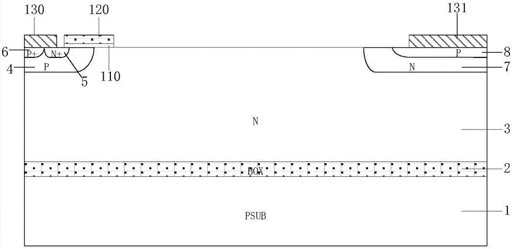
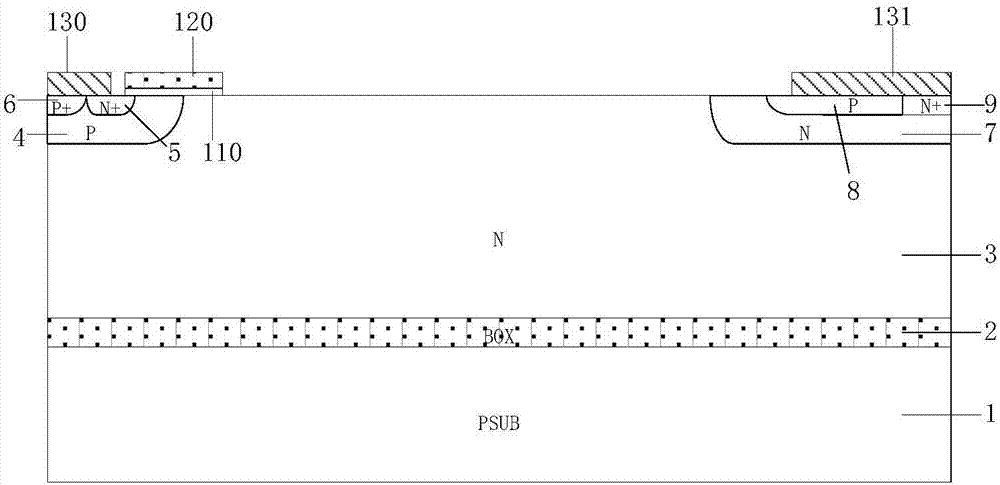
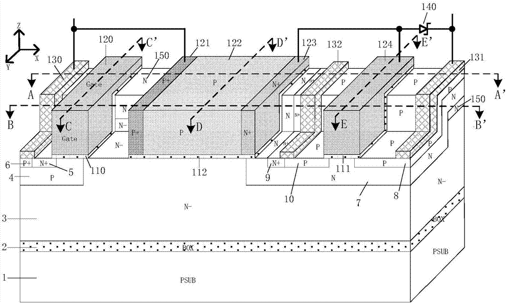
[0035] Such as image 3 As shown, it is a schematic structural diagram of this example, and its half-cell structure includes a substrate 1, an insulating layer 2, and a first N-type low-doped region 3 stacked in sequence from bottom to top; it is characterized in that, along the longitudinal direction of the device, The first N-type low-doped region 3 is in the shape of a two-level ladder, and the vertical height of the second-level step is defined to be greater than the first-level step. Both sides of the upper layer of the first N-type low-doped region 3 have P-type bodies respectively. Region 4 and N-type buffer zone 7, along the longitudinal direction of the device, the P-type body region 4 and N-type buffer zone 7 are two-level ladder; in the first N-type low-doped region 3 second-level ladder and P There is a second N-type low-doped region 150 between the second level of the N-type body region 4 and the N-type buffer zone 7; the upper layer of the P-type body region 4 ha...

Embodiment 2

[0042] Such as Figure 9 As shown, different from Example 1,

[0043] A zener diode is directly formed in the polysilicon layer above the dielectric layer 112, the zener diode is formed on the device surface between the trenches, the P+ region 125 is the anode of the zener diode, and the N+ region 126 is the cathode of the zener diode . The type, location and shape of the Zener diodes can be adjusted as desired.

Embodiment 3

[0045] Such as Figure 10 As shown, the difference from Embodiment 1 is that a Zener diode is directly formed in the polysilicon layer above the dielectric layer 111, and the Zener diode is formed on the surface of the device between the trenches, and the P+ region 125 is a Zener diode The anode of the N+ region 126 is the cathode of the Zener diode. The type, location and shape of the Zener diodes can be adjusted as desired.


PUM


Abstract

The invention belongs to the technical field of a semiconductor power device, and specifically relates to a lateral insulated gate bipolar transistor. On the basis of a conventional lateral insulated gate bipolar transistor structure, trench etching is performed in the surface of a device in a channel length direction to form a three-dimensional structure and to form the lateral insulated gate bipolar transistor with the three-dimensional structure; and meanwhile, a polycrystal diode is formed on the surface of a three-dimensional drift region of the device, and a three-dimensional PMOS and a zener diode are integrated close to a collector. The lateral insulated gate bipolar transistor has a lower forward conduction voltage drop compared with the conventional LIGBT, without causing a negative impedance phenomenon in the conduction process; and meanwhile, the lateral insulated gate bipolar transistor has higher device breakdown voltage, higher switching-off speed and lower switching-off loss.

Description

technical field [0001] The invention belongs to the technical field of semiconductor power devices, and in particular relates to a lateral insulated gate bipolar transistor. Background technique [0002] Insulated gate bipolar transistor (IGBT) is a new type of power electronic device combined with MOS field effect and bipolar transistor. The advantages of large current and low loss have become the mainstream power switching devices in the field of medium and high power power electronics, and are widely used in various fields of the national economy such as communications, energy, transportation, industry, medicine, household appliances, and aerospace. Internationally well-known semiconductor companies, such as ABB, Infineon (IR), ST, Renesas, Mitsubishi, FuJi, etc. have successively invested in the R&D and manufacturing of IGBTs. In recent years, as a hot field of power electronics, IGBT has received great attention from developed countries and regions such as the United S...

Claims


Application Information

Patent Timeline
Patent Type & Authority Applications(China)
IPC IPC(8): H01L29/739H01L27/06
CPCH01L27/0629H01L29/7394
Inventor 张金平陈钱刘竞秀李泽宏任敏张波
Owner UNIV OF ELECTRONICS SCI & TECH OF CHINA
Why Eureka
Try Eureka